Inside a Charger: PCB, IC, Transformer Explained (How Modern Fast Chargers Really Work)
⭐ Featured Snippet
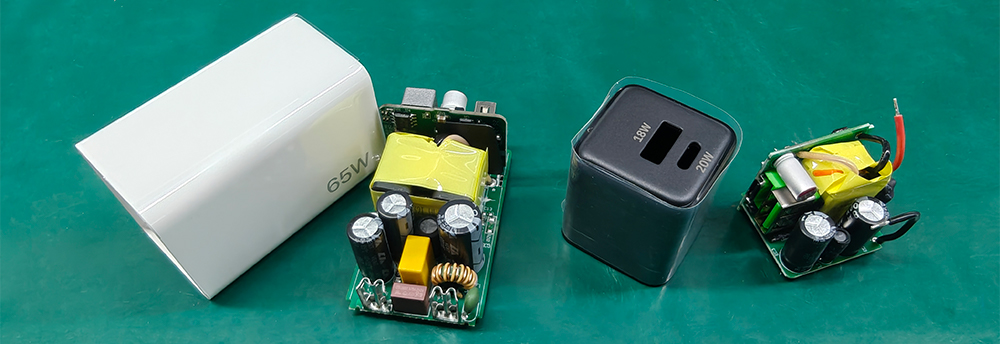
Inside a modern charger are several key components including the PCB (Printed Circuit Board), power IC, transformer, capacitors, and MOSFETs. These parts work together to convert AC wall power into stable DC power for phones, laptops, and USB-C fast charging devices. The quality of these internal components directly affects charging speed, safety, heat control, and efficiency.
Introduction
Most people only see the outside of a charger:
• a USB-C port
• a compact plastic shell
• a wattage label like 20W, 65W, or 140W
But inside that small adapter is an incredibly sophisticated power system.
Modern chargers are no longer simple “power bricks.”
Today's:
• USB-C PD chargers
• GaN chargers
• PPS chargers
• laptop chargers
• phone chargers
…contain high-speed power conversion circuits operating thousands—or even millions—of times per second.
And at the center of this system are three critical components:
👉 PCB
👉 Power IC
👉 Transformer
Understanding these parts is essential for evaluating charger quality, safety, efficiency, and fast charging performance.
Two chargers may both claim:
• 65W
• USB-C PD
• GaN fast charging
…but internally they can be completely different.
A high-quality charger offers:
✔ stable voltage
✔ lower heat
✔ longer lifespan
✔ safer charging
✔ higher efficiency
While poor internal engineering can cause:
❌ overheating
❌ unstable charging
❌ power drops
❌ shortened product life
👉 This is why professional charger manufacturers and OEM charger factories invest heavily in internal component design.
The Main Components Inside a Modern Charger
A modern charger usually contains:
| Component | Function |
| PCB | Connects and controls all circuits |
| Power IC | Controls charging behavior |
| Transformer | Converts voltage |
| Capacitors | Smooth power output |
| MOSFETs | High-speed switching |
| Rectifier | Converts AC to DC |
| Thermal Materials | Reduce heat buildup |
1. What Is the PCB Inside a Charger?
PCB stands for:
👉 Printed Circuit Board
It is the structural and electrical foundation of the charger.
What the PCB Actually Does
The PCB:
• connects all electronic components
• routes electrical signals
• manages high-voltage and low-voltage separation
• affects thermal performance
Think of it as:
👉 the “city infrastructure” inside the charger.
Without the PCB:
• components cannot communicate
• electricity cannot flow properly
Why PCB Quality Matters in Fast Chargers
Fast charging creates:
• high current
• high switching frequency
• significant heat
Poor PCB design can lead to:
❌ unstable voltage
❌ overheating
❌ efficiency loss
Professional PCB Engineering Includes
• thicker copper layers
• optimized trace routing
• thermal isolation zones
• EMI shielding design
👉 Premium PD charger factories and laptop charger manufacturers often use multi-layer PCBs to improve stability.
PCB in GaN Chargers
GaN chargers are extremely compact.
This means PCB layout becomes even more critical because:
• components are tightly packed
• thermal density is high
• switching frequency is faster
👉 This is why advanced GaN charger manufacturers focus heavily on PCB thermal engineering.
2. What Is the Power IC in a Charger?
The IC (Integrated Circuit) is essentially:
👉 the “brain” of the charger.
It controls:
• voltage regulation
• current output
• fast charging protocols
• temperature protection
• device communication
How the Power IC Enables Fast Charging
Modern USB-C chargers support:
• PD3.0
• PD3.1
• PPS fast charging
• QC fast charging
The IC constantly communicates with your device to determine:
• how much voltage to supply
• how much current is safe
• when to reduce charging speed
Example
A Samsung phone may request:
• 9V / 3A PPS charging
A laptop may request:
• 20V / 5A PD3.1 charging
The IC dynamically manages this entire process in real time.
Why Cheap ICs Cause Problems
Low-quality IC chips may result in:
❌ unstable charging
❌ charging disconnects
❌ overheating
❌ protocol compatibility issues
👉 This is why experienced phone charger manufacturers prioritize branded, high-performance controller ICs.
Smart Protection Features Controlled by ICs
Modern charger ICs also manage:
✔ over-voltage protection
✔ over-current protection
✔ short-circuit protection
✔ thermal shutdown
✔ power balancing
Without intelligent IC control, fast charging would be dangerous.
3. What Does the Transformer Do Inside a Charger?
The transformer is one of the most important components in any:
• AC to DC adapter
• wall charger
• laptop charger
• USB charger
Main Function
The transformer changes voltage levels safely.
For example:
• wall AC input → high voltage
• charger output → low-voltage DC
Why Transformers Generate Heat
Transformers work using:
• electromagnetic induction
• high-frequency switching
This naturally creates heat through:
• copper losses
• magnetic core losses
• eddy currents
Modern Fast Chargers Use High-Frequency Transformers
Today's fast chargers use:
• smaller transformers
• higher switching frequencies
Benefits:
✔ smaller charger size
✔ faster response
✔ higher power density
But this also increases engineering difficulty.
Why GaN Chargers Can Use Smaller Transformers
GaN technology enables:
• faster switching
• higher frequency operation
This allows transformers to shrink dramatically.
👉 That's why a modern:
• 65W charger
• 100W USB-C charger
• 140W PD3.1 charger
…can now fit in your pocket.
Capacitors: The Power Smoothers
Capacitors help:
• smooth voltage ripple
• stabilize output
• reduce electrical noise
In fast charging systems, poor capacitors can cause:
❌ unstable charging
❌ power fluctuation
❌ shortened charger lifespan
High-quality USB charger factories usually select long-life capacitors rated for:
• high temperature
• low ESR
• extended durability
MOSFETs: The High-Speed Switching Engine
MOSFETs rapidly switch electricity on and off.
This creates:
• efficient power conversion
• voltage regulation
• fast charging control
However: MOSFETs are also one of the biggest heat sources inside a charger.
Why Charger Thermal Design Is Critical
Modern fast chargers process enormous power in tiny spaces.
Examples:
• 20W charger / 45W charger / 65W charger / 100W charger / 140W charger
Without proper thermal management:
❌ temperatures rise rapidly
❌ efficiency drops
❌ component lifespan decreases
How Professional Charger Factories Reduce Heat
Professional PD charger factories and charger type-C manufacturers optimize:
• PCB copper thickness
• transformer spacing
• airflow paths
• thermal pads
• GaN efficiency tuning
👉 The best charger engineering is often invisible from the outside.
Zonsan Fast Charger Factory Engineering Insight
As a professional charger manufacturer, Zonsan Power places strong emphasis on internal structural engineering.
From compact 20W USB-C chargers to advanced 140W PD3.1 GaN laptop chargers, Zonsan engineers optimize:
• PCB layout
• transformer efficiency
• thermal balance
• protocol IC tuning
to improve charging stability, safety, and long-term reliability.
Why Internal Components Determine Charger Quality
The real difference between a cheap charger and a premium charger is often hidden internally.
Better components lead to:
✔ cooler temperatures
✔ higher efficiency
✔ stable fast charging
✔ better compatibility
✔ longer product life
This is especially important for:
• iPhone charger factory products
• Samsung S26 charger factory solutions
• MacBook charger designs
• PPS charger factory manufacturing
The Future of Charger Engineering
Future chargers are moving toward:
• AI thermal control
• digital power management
• GaN + SiC hybrid systems
• ultra-high efficiency conversion
• higher-density PCB design
The next generation of USB-C charger manufacturers will compete not only on wattage—but also on:
✔ thermal engineering
✔ internal architecture
✔ efficiency optimization
✔ smart IC control
Final Verdict
Inside every modern charger is a complex power conversion system built around:
👉 PCB
👉 IC
👉 Transformer
These components work together to deliver:
• safe charging
• stable voltage
• high efficiency
• intelligent fast charging
And in today’s fast-charging world, the quality of those internal components matters more than ever.
FAQ (People Also Ask)
Q1: What is the PCB inside a charger?
The PCB is the main circuit board that connects and controls all charger components.
Q2: What does the IC do in a charger?
The IC controls voltage, current, fast charging protocols, and safety protection.
Q3: Why does a charger need a transformer?
The transformer safely converts voltage levels for charging devices.
Q4: What component generates the most heat inside a charger?
Usually the MOSFETs and transformer.
Q5: Why are GaN chargers smaller?
GaN semiconductors switch faster, allowing smaller transformers and compact designs.
Q6: Can poor internal components damage devices?
Yes. Low-quality components may cause unstable power or overheating.
Q7: Why do premium chargers cost more?
They use higher-quality components, better PCB design, and advanced thermal engineering.
Q8: What is the role of capacitors in a charger?
Capacitors smooth voltage and stabilize output power.