From PCB Design to Mass Production: How a Charger Is Developed
When people see a finished GaN charger, it often looks simple.
A compact housing.
A USB-C port.
Maybe a folding plug.
But behind that small device is a long engineering process involving:
• Electronic architecture
• PCB design
• Thermal simulation
• Protocol debugging
• Reliability testing
• Safety certification
• Production optimization
Modern fast chargers are no longer simple power adapters.
Today's USB-C PD chargers, PPS chargers, and GaN chargers operate more like miniature intelligent power systems.
Especially for:
• 65W laptop chargers
• 100W multi-port chargers
• 140W PD3.1 chargers
• AI laptop chargers
• Desktop charging stations
engineering complexity has increased dramatically.
In this article, we will walk through how a modern charger is actually developed — from initial concept to mass production — and explain why charger R&D has become one of the biggest competitive advantages in the fast charging industry.
Step 1 — Defining the Charger Architecture
Every charger project starts with defining the product architecture.
Before PCB design begins, engineers must determine:
• Output power
• Port configuration
• USB-C PD support
• PPS compatibility
• Thermal limitations
• Size targets
• Safety requirements
For example:
A compact 35W GaN charger has very different engineering priorities compared with a 140W desktop charger.
A smartphone charger may prioritize:
• Small size
• Portability
• Low temperature
• Folding plug design
while a high-power laptop charger may prioritize:
• Sustained output stability
• Multi-device charging
• Thermal management
• PD3.1 AVS compatibility
At this stage, engineers also evaluate:
• GaN vs silicon architecture
• Transformer size
• Power topology
• Efficiency targets
• Heat dissipation paths
These early decisions directly affect the entire development process later.
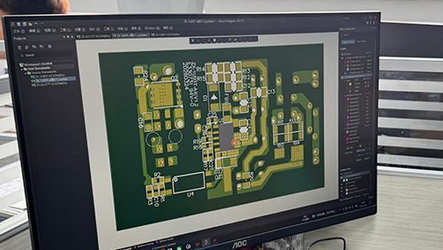
Once the charger architecture is finalized, PCB development begins.
PCB layout is one of the most important parts of charger engineering.
Inside modern GaN chargers, PCB space is extremely limited while power density continues increasing.
Engineers must carefully optimize:
• Power routing
• High-voltage isolation
• Thermal balance
• Signal integrity
• EMI suppression
• USB-C PD communication
A poorly designed PCB can eventually create:
• Excessive heat
• PD instability
• Coil noise
• Reduced efficiency
• Safety risks
• Shortened lifespan
For high-power chargers, even component placement distance becomes extremely important.
Modern charger PCB development often involves multiple engineering revisions before final approval.
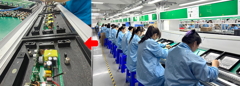
Step 3 — Prototype Development and Debugging
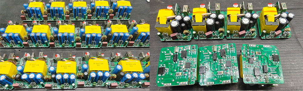
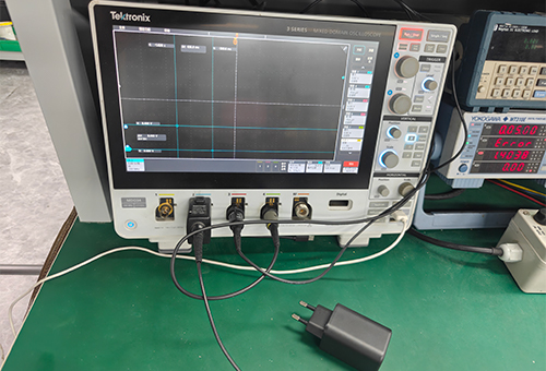
After PCB design is completed, engineers produce prototype boards for testing.
This is where the charger begins moving from theory into real hardware.
Prototype debugging often reveals unexpected engineering challenges such as:
• Thermal hotspots
• PD handshake instability
• EMI interference
• Transformer noise
• Power fluctuation
• Component overheating
Engineers use equipment including:
• Oscilloscopes
• Thermal cameras
• USB-C protocol analyzers
• Electronic loads
• EMI testing systems
to continuously optimize charger behavior.
In many projects, multiple prototype revisions are required before the design becomes stable enough for certification and production.
Step 4 — Thermal Engineering Optimization
Heat management is one of the biggest challenges in modern charger development.
This is especially true for compact high-power GaN chargers.
Today’s 100W and 140W chargers generate significant internal heat because of:
• High switching frequency
• Dense PCB layouts
• Multi-port charging
• Compact housing size
Thermal engineering therefore becomes a critical part of charger R&D.
Engineers optimize:
• Transformer positioning
• Thermal pad placement
• Airflow paths
• PCB copper thickness
• Housing ventilation
• Heat transfer efficiency
In some cases, even small internal structural changes can reduce charger temperature significantly.
Good thermal design directly improves:
• Reliability
• Safety
• Charging stability
• Product lifespan
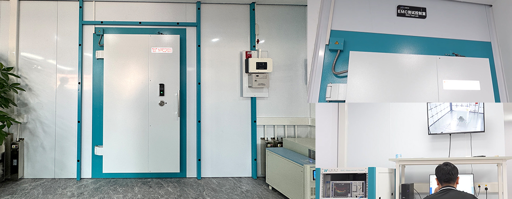
Step 5 — Safety and Certification Preparation
Before mass production begins, chargers must pass multiple safety and compliance tests.
Depending on the target market, products may require:
• CE certification
• FCC certification
• RoHS compliance
• KC certification
• ETL certification
• ERP requirements
At this stage, engineers verify:
• Insulation distance
• Leakage current
• Temperature rise
• EMI emissions
• Electrical stability
• Protection system behavior
Products that fail certification testing often require PCB redesign or structural modification.
This is why certification engineering is closely tied to product development itself.
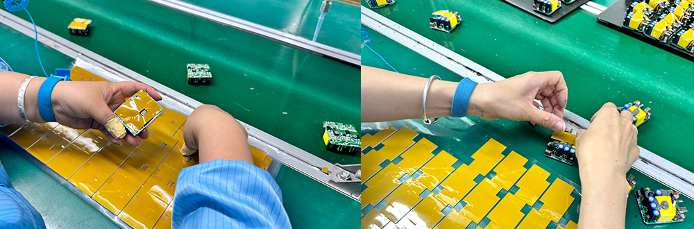
Step 6 — Trial Production and Manufacturing Optimization
Once engineering validation is completed, the project enters trial production.
This stage helps engineers verify whether the charger can be manufactured consistently at scale.
Factories evaluate:
• SMT production stability
• Assembly efficiency
• Yield rate
• Thermal consistency
• Solder quality
• Production speed
Many engineering adjustments actually happen during trial production rather than earlier prototype stages.
Professional charger factories continuously optimize manufacturing processes before large-scale production begins.
This stage is critical because a design that works in small quantities may still fail during mass production.
Step 7 — Mass Production and Reliability Verification
After all engineering stages are completed, the charger enters mass production.
However, development does not stop here.
Professional charger manufacturers continue monitoring:
• Production consistency
• Failure rates
• Thermal behavior
• Aging test results
• Customer feedback
• Reliability performance
Continuous engineering optimization remains important throughout the entire product lifecycle.
This is especially important for OEM and ODM projects where long-term product stability directly affects brand reputation.
Why Charger Development Is Becoming More Complex
The fast charging industry is evolving rapidly.
Future chargers are becoming:
• Smaller
• More powerful
• Multi-device compatible
• AI-device optimized
• Thermally denser
This means charger development is becoming increasingly engineering-intensive.
Modern charger R&D now combines:
• Power electronics
• Thermal engineering
• Software protocols
• Manufacturing engineering
• Reliability science
• Safety compliance
The factories that invest deeply in engineering capability will have a major advantage in future charging technology.
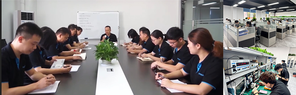
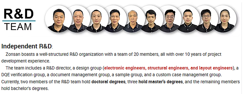
How ZONSAN Develops USB-C Fast Chargers
As a professional charger manufacturer with 16 years of experience, ZONSAN continuously invests in charger engineering, thermal optimization, and power architecture development.
The company’s R&D team focuses on:
• USB-C PD stability
• PPS charging optimization
• Multi-port power allocation
• Thermal management
• Compact GaN architecture
• Reliability engineering
ZONSAN develops various charging products including:
• 20W USB-C chargers
• 35W GaN chargers
• 65W laptop chargers
• 100W PD chargers
• 140W PD3.1 chargers
• PPS fast chargers
• Desktop charging stations
for OEM and ODM customers worldwide.
The engineering team continuously improves PCB layouts, thermal structures, and charging stability to support modern smartphones, tablets, laptops, and AI computing devices.
Final Thoughts
Behind every reliable fast charger is a long engineering process that most consumers never see.
From PCB design and thermal optimization to protocol debugging and reliability verification, modern charger development has become far more complex than many people realize.
As charging technology continues evolving toward higher power and smaller form factors, engineering capability will become one of the biggest differences between professional charger manufacturers and low-cost suppliers.
Because in the future of USB-C charging, the real competition is no longer only about wattage.
It is about engineering.
FAQ
Q1: How is a USB-C charger developed?
A: A USB-C charger is developed through multiple stages including architecture planning, PCB design, prototype testing, thermal optimization, certification testing, and mass production validation.
Q2: Why is PCB design important for chargers?
A: PCB design directly affects thermal performance, charging stability, efficiency, EMI behavior, and long-term reliability.
Q3: Why do GaN chargers require more engineering?
A: GaN chargers operate at higher switching frequencies and power density, requiring more advanced thermal design and PCB optimization.
Q4: What happens during charger prototype testing?
A: Engineers test thermal behavior, PD protocol communication, power stability, EMI emissions, and reliability performance.
Q5: Why do some chargers overheat more easily?
A: Poor PCB layout, weak thermal design, low-quality components, or insufficient engineering optimization can all increase charger temperature.
Q6: What certifications do chargers need?
A: Depending on the market, chargers may require CE, FCC, RoHS, KC, ETL, ERP, or other safety certifications.
Q7: Why is trial production important?
A: Trial production helps verify manufacturing stability, yield rate, thermal consistency, and large-scale production reliability.
Q8: What makes a professional charger factory?
A: Professional charger factories invest heavily in R&D engineering, SMT precision, thermal testing, reliability verification, and production optimization.