Inside a GaN Charger Production Line: From PCB to Final Assembly
When most people look at a GaN charger, they only see a small white charging block. But inside that compact housing is a surprisingly complex engineering system involving PCB layout design, thermal architecture, SMT precision manufacturing, aging tests, safety verification, and automated assembly processes.
In recent years, demand for USB-C fast chargers, PD3.1 chargers, PPS chargers, laptop chargers, and multi-port GaN chargers has increased rapidly across Europe, South Korea, and North America. As charging power continues rising from 20W and 45W to 100W, 140W, and even 240W, manufacturing standards inside charger factories have also changed dramatically.
Modern charger production is no longer simple electronic assembly. It is now a highly engineered manufacturing process where thermal control, power efficiency, safety protection, and reliability testing all directly affect product quality.
This article takes you inside a real GaN charger production line — from PCB manufacturing to final assembly and testing — to explain how high-quality USB-C chargers are actually built.
Why GaN Chargers Require More Advanced Manufacturing
Compared with traditional silicon chargers, GaN chargers operate at much higher switching frequencies and power densities. This allows chargers to become smaller, faster, and more efficient, but it also makes engineering and manufacturing far more demanding.
A low-quality production process can easily create problems such as:
• Excessive heat
• Unstable charging
• USB-C PD handshake failures
• Coil noise
• Poor thermal dissipation
• Shortened product lifespan
• Safety risks during high-power charging
This is especially critical for modern 65W, 100W, 140W, and PD3.1 AVS chargers used for MacBook, gaming laptops, tablets, Samsung Galaxy devices, and AI laptops.
For this reason, professional charger manufacturers now invest heavily in SMT precision, thermal engineering, automated testing systems, and reliability verification.
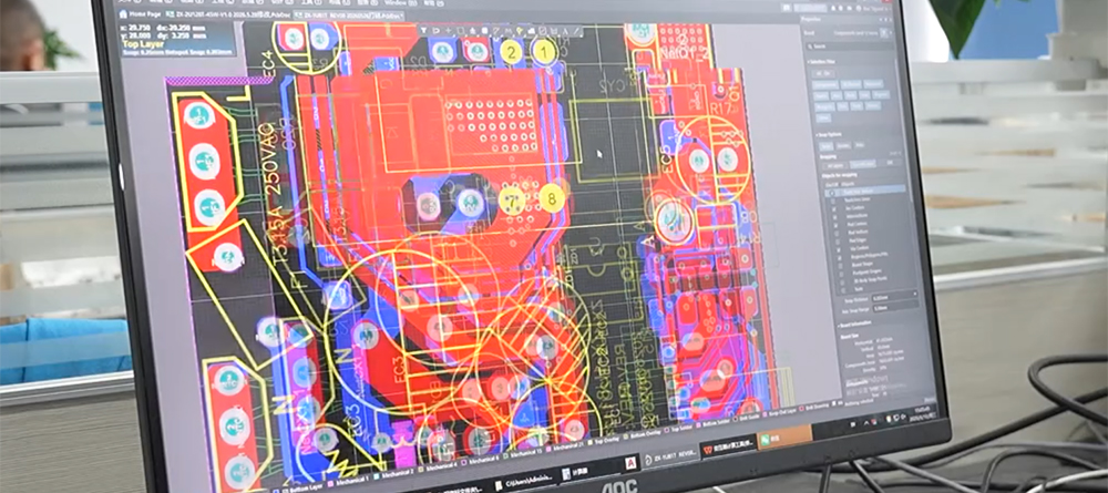
Step 1 — PCB Design and Engineering Verification
Every charger starts with PCB engineering.
Before production begins, engineers must design the charger’s internal power architecture based on:
• Output power requirements
• USB-C PD protocols
• PPS voltage range
• Thermal performance
• Component spacing
• EMI suppression
• Safety certification requirements
For a modern GaN charger, PCB layout becomes especially important because internal space is extremely limited.
Poor PCB design can lead to:
• Higher temperatures
• Signal interference
• Lower efficiency
• Unstable power delivery
• Increased failure rates
This is why high-end PD charger factories often spend weeks optimizing PCB traces, transformer positioning, heat dissipation paths, and IC layouts before mass production begins.
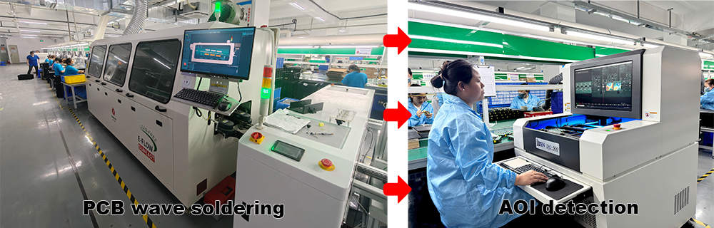
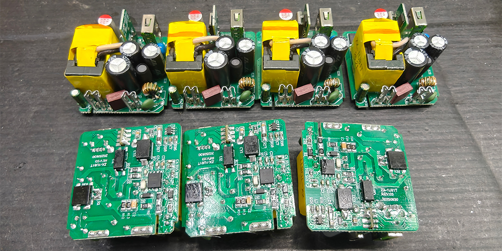
Step 2 — SMT Production (Surface Mount Technology)
After PCB verification is completed, production moves into SMT manufacturing.
This is one of the most critical stages inside a USB charger factory.
SMT machines automatically place miniature electronic components onto the PCB at extremely high speed and precision. Components include:
• GaN power ICs
• MOSFETs
• Capacitors
• Transformers
• USB-C controllers
• PD protocol ICs
• Synchronous rectifiers
For high-power GaN chargers, SMT accuracy directly affects charging stability and thermal reliability.
Even microscopic soldering defects may eventually cause:
• Charger overheating
• Intermittent charging
• Voltage instability
• Reduced lifespan
Modern charger factories therefore use AOI (Automated Optical Inspection) systems after SMT placement to inspect solder quality and component alignment.
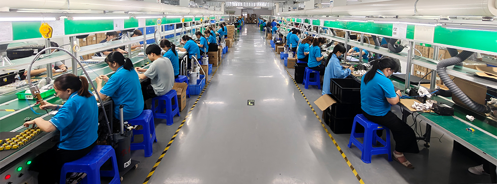
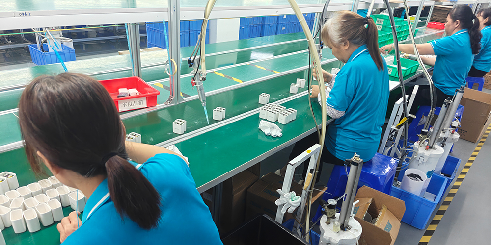
Step 3 — Transformer Assembly and Manual Engineering Processes
Although charger production is highly automated today, some critical processes still require skilled manual assembly.
Transformer installation is one example.
Inside a fast charger, the transformer plays a major role in voltage conversion and power transfer efficiency. Improper transformer assembly can create excessive heat, electromagnetic interference, or unstable charging performance.
In many professional charger factories, engineers also manually inspect:
• Thermal pads
• Insulation materials
• Solder joints
• Potting areas
• High-voltage spacing
• Internal cable routing
This becomes even more important for compact multi-port GaN chargers where internal spacing is extremely tight.
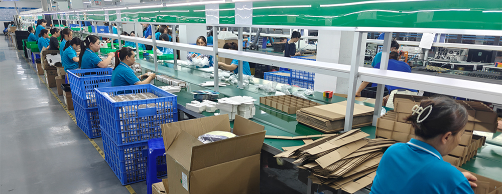
Step 4 — Housing Assembly and Safety Protection
Once the internal PCB is completed, the charger moves to final assembly.
The housing design of a charger is not only cosmetic. It also affects:
• Heat dissipation
• Structural strength
• Fire resistance
• User safety
• Port durability
For modern USB-C wall chargers, manufacturers often use flame-retardant PC materials that meet CE, FCC, RoHS, KC, or ETL safety standards.
At this stage, factories also verify:
• USB-C port alignment
• Plug stability
• Housing sealing
• Surface finish quality
• Logo printing accuracy
For OEM charger manufacturers, this stage is also where customized branding and packaging are integrated into production.
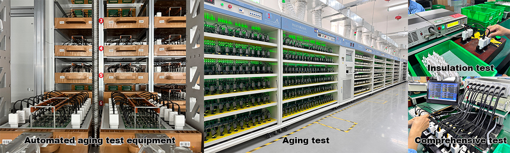
Step 5 — Aging Test and Reliability Verification
Before shipping, professional charger manufacturers perform aging tests on every production batch.
This is one of the most important quality control stages inside a charger factory.
During aging tests, chargers operate continuously under controlled temperatures and electrical loads for several hours or even days.
The purpose is to detect:
• Early component failures
• Thermal instability
• Voltage fluctuations
• Abnormal shutdowns
• USB-C PD negotiation failures
For high-power chargers such as 100W and 140W GaN chargers, aging tests become especially critical because thermal stress is much higher than in traditional chargers.
Reliable OEM charger factories also perform additional tests including:
• Hi-pot testing
• Drop testing
• Short-circuit testing
• Over-current testing
• Temperature rise testing
• EMI testing
Why Production Quality Matters More Than Specifications
Today, many chargers on the market advertise similar specifications:
• 100W PD charger
• PPS fast charging
• GaN technology
• Multi-port charging
But real-world reliability often depends less on marketing specifications and more on manufacturing quality.
A well-engineered charger typically includes:
• Better thermal architecture
• Higher-quality capacitors
• More stable PCB layouts
• Improved insulation
• Better solder consistency
• More complete testing procedures
This is why two chargers with identical power ratings can perform very differently in long-term usage.
Professional charger manufacturers understand that reliability is built during production — not only during product design.

As a professional charger manufacturer with 16 years of experience, ZONSAN focuses heavily on engineering reliability and manufacturing consistency for USB-C fast chargers, PD chargers, PPS chargers, desktop chargers, and high-power GaN charging solutions.
The factory's engineering team continuously optimizes:
• PCB thermal architecture
• USB-C PD stability
• Multi-port power allocation
• Aging test procedures
• Production consistency
ZONSAN's production system also integrates SMT manufacturing, automated testing equipment, aging verification, and multiple safety inspection stages to improve long-term charger reliability for OEM and ODM customers worldwide.
Final Thoughts
A modern GaN charger may look simple from the outside, but behind that compact design is a highly engineered manufacturing process involving PCB design, thermal management, SMT precision, safety testing, and reliability verification.
As charging technology continues evolving toward higher power, smaller sizes, and AI-device compatibility, charger manufacturing standards will become even more demanding.
For this reason, choosing an experienced charger factory is no longer only about price. It is increasingly about engineering capability, manufacturing consistency, and long-term reliability.
The future of USB-C charging will not only be defined by faster charging speeds — but by better engineering behind every charger.
FAQ - Gan Charger Manufacturer
Q1: What is SMT in charger manufacturing?
A: SMT (Surface Mount Technology) is the automated process of placing electronic components onto a PCB using high-speed machines. It is one of the most important stages in fast charger manufacturing.
Q2: Why do GaN chargers require more advanced production?
A: GaN chargers operate at higher switching frequencies and power densities, making thermal design, PCB layout, and manufacturing precision much more critical.
Q3: What is an aging test for chargers?
A: An aging test runs chargers continuously under electrical load for extended periods to identify early failures and verify long-term reliability.
Q4: Why do some chargers overheat more easily?
A: Overheating is often caused by poor thermal design, low-quality components, insufficient testing, or unstable PCB layouts.
Q5: How are USB-C PD chargers tested?
A: Professional charger factories perform multiple tests including aging tests, thermal testing, EMI testing, short-circuit testing, and PD protocol verification.
Q6: What components inside a charger affect quality the most?
A: Important components include the transformer, capacitors, GaN ICs, MOSFETs, thermal materials, and PCB layout quality.
Q7: Why are high-power chargers harder to manufacture?
A: High-power chargers generate more heat and require more advanced thermal architecture, power management, and reliability testing.
Q8: What should OEM buyers look for in a charger factory?
A: OEM buyers should evaluate engineering capability, certification compliance, testing procedures, SMT quality control, and production consistency.