How an Advanced Charger PCB Improves Fast Charging Efficiency
—— Inside a Fast Charger: How Advanced PCB Design Boosts Efficiency and Safety
Modern mobile phone chargers do much more than simply “plug and charge.” Behind every efficient fast charger lies a highly optimized circuit board (PCB) that enables stable power conversion, supports smart charging protocols, and reduces heat generation — all critical for delivering power safely and quickly to 2026’s high-performance smartphones and tablets.
In this guide, we explain how advanced PCB designs transform charging efficiency for modern devices and what features matter most in today’s USB-C fast chargers.
What Is a Charger PCB and Why It Matters
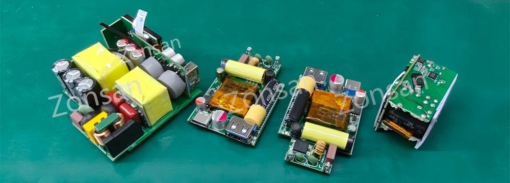
A charger PCB (Printed Circuit Board) is the central backbone of any mobile phone charger, where all power components, control ICs, semiconductor devices, and safety circuits are assembled. It determines how well the charger can convert electrical power and manage heat, noise, and multiple charging standards.
A poorly designed PCB can lead to:
· Low power density
· Higher operating temperatures
· Inefficient power delivery
· Reduced support for fast charging protocols
An optimized PCB, on the other hand, ensures high efficiency, stable performance, and long-term reliability.
Step-by-Step: How a Charger PCB Improves Efficiency
1. High-Density Layout and Component Placement
Advanced charger PCBs are often multi-layer designs with compact routing to support higher power density and efficiency. This minimizes trace length and reduces energy loss. Tight layout control also improves thermal dissipation, which helps maintain stable output under load.
2. Optimized Power Conversion Stages
Most modern fast charger PCBs support switching regulators and power stages that handle DC-DC conversion with minimal loss. High-frequency switching lets the board use smaller inductors and capacitors, shrinking total PCB area while retaining efficiency.
3. USB-C and Fast Charging Protocol Integration
Implementing USB Power Delivery (PD) and other protocols such as QC 4+ on the PCB requires careful routing of communication lines (CC1/CC2) and inclusion of dedicated PD controller ICs. These chips manage the handshake between the charger and the device, enabling dynamic voltage and current negotiation for faster charging.
4. Thermal and Safety Control
Efficient PCB design includes thermal vias, copper pours, and optimized power planes that carry current without overheating. Safety circuits like Over-Voltage Protection (OVP), Over-Current Protection (OCP), and temperature monitoring are integrated into the board layout to protect both the charger and the connected device.
Why PCB Design Matters for GaN and High-Efficiency Chargers
The rise of GaN (Gallium Nitride) devices has pushed charger performance even further. GaN technology enables higher switching frequencies and lower conduction losses compared with silicon, but it also demands good PCB layout practices to maximize efficiency.
• GaN chargers can reduce transformer size and heat buildup due to less energy wasted as heat.
• Higher switching frequency means components can be placed closer together on the PCB, yielding a smaller overall charger footprint.
In essence, a well-designed PCB unlocks the full potential of GaN and modern power components, enabling fast chargers to deliver power efficiently even at high wattages like 65W, 100W, or more.
Real-World Benefits of PCB-Driven Efficiency
An advanced charger PCB translates directly into better user experience:
• Faster charging times for phones, tablets, and laptops
• Lower operating temperatures for longer charger life
• More compact charger designs without performance loss
• Stable output during heavy use
• Improved support for multi-device charging via intelligent power allocation
These improvements are why modern fast chargers have become smaller, cooler, and more powerful than older designs.
Choosing Chargers With Advanced PCB Designs
When selecting a charger — whether a consumer brand or a supplier from a charger factory — look for:
• Clear support for USB Power Delivery (PD) and PPS
• Evidence of multi-layer PCB designs for power density
• Efficient thermal management (copper pours, vias)
• Certifications like CE, FCC, RoHS
• Use of efficient devices like GaN transistors
A charger with these PCB features delivers real fast charging performance, not just marketing claims.
FAQ — Charger PCB and Efficiency
Q: What role does a PCB play in fast chargers?
A: It provides the structural and electrical foundation where power components and control ICs are placed, impacting power conversion efficiency and thermal behavior.
Q: Why are USB-C fast chargers more efficient than older chargers?
A: USB-C PD chargers use advanced PCBs and controllers that negotiate power dynamically, reducing energy loss and improving overall efficiency.
Q: Is GaN technology better for PCB design?
A: Yes. GaN enables higher switching frequency and lower losses, allowing smaller PCB layouts and cooler operation.
Q: How many layers do advanced charger PCBs typically use?
A: High-efficiency chargers often use 4–6+ layer PCBs to support dense routing, shielding, and thermal management.
Q: Does PCB layout affect charger safety?
A: Absolutely. A good PCB design integrates safety protections (OVP, OCP, OTP) and efficient heat paths to prevent failures.