Why Charger PCB Design Determines Fast Charging Performance
• wattage
• GaN technology
• charging protocols
• USB-C ports
But inside every modern charger lies one of the most important engineering components:
the PCB.
The PCB (Printed Circuit Board) is essentially: the nervous system of a charger.
It controls:
• power flow
• signal communication
• thermal behavior
• voltage regulation
• EMI suppression
• charging stability
In fact, two chargers using the exact same components can still perform very differently because of: PCB design quality.
This is especially true for:
• 65W chargers
• 100W GaN chargers
• PD3.1 desktop chargers
• multi-port USB-C charging stations
where internal power density becomes extremely high.
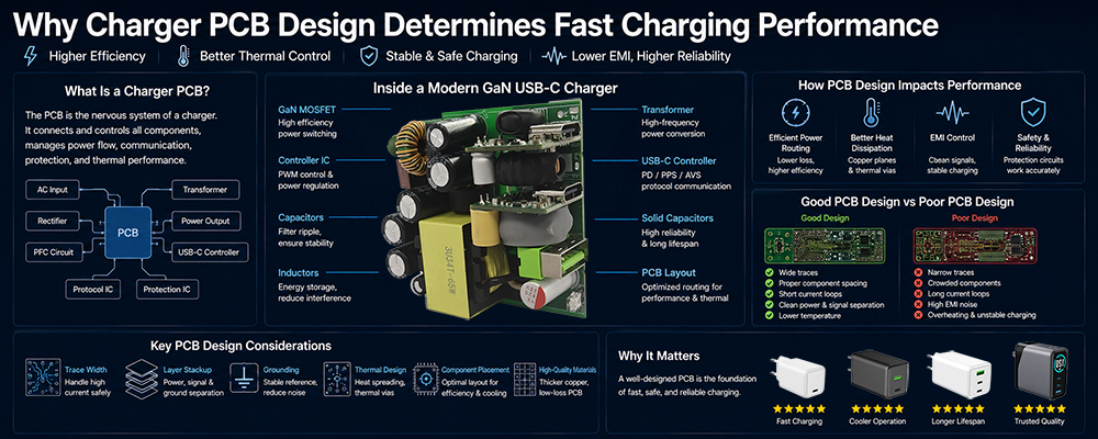
What Is a Charger PCB?
A PCB (Printed Circuit Board) is the internal board that electrically connects all charger components together.
This includes:
• transformers
• capacitors
• MOSFETs
• protocol ICs
• rectifiers
• USB-C controllers
• thermal sensors
The PCB determines how electricity moves throughout the charger.
In modern fast chargers, PCB design directly affects:
• efficiency
• charging speed
• temperature
• reliability
• EMI performance
• long-term durability
Why PCB Design Became More Important in the GaN Era
Traditional silicon chargers operated at:
• lower switching frequencies
• lower power density
which made PCB layout somewhat more forgiving.
But modern GaN chargers operate at:
• much higher switching speeds
• significantly denser internal layouts
• higher thermal concentration
This creates: far stricter PCB engineering requirements.
Poor PCB design in GaN chargers may cause:
• excessive heat
• unstable charging
• EMI problems
• protocol instability
• reduced efficiency
Why High-Wattage Chargers Need Better PCB Engineering
As chargers move from:
• 20W
to:
• 65W / 100W / 140W / 240W PD3.1 systems
internal current flow increases dramatically.
Higher current means:
• more heat
• stronger electromagnetic interference
• tighter spacing challenges
• higher thermal stress
This is why professional charger manufacturers spend enormous effort optimizing: PCB layouts.
How PCB Layout Affects Charging Efficiency
Electricity flowing through PCB traces creates resistance.
Poor routing design can increase:
• power loss
• thermal buildup
• voltage instability
Good PCB layouts reduce:
• resistance
• signal noise
• unnecessary power loss
which improves: charging efficiency.
Even small efficiency gains become extremely important in:
• compact GaN chargers
• high-density desktop chargers
• multi-port USB-C systems
Why PCB Trace Width Matters
PCB traces act like electrical highways.
If traces are too narrow:
• resistance increases
• temperature rises
• voltage drops become worse
High-power chargers therefore require:
• wider power traces
• optimized copper thickness
• controlled current distribution
especially in:
• 100W+
• 140W
• 240W PD3.1 chargers
Why PCB Layer Structure Is Important
Modern fast chargers often use: multi-layer PCBs.
Additional layers help separate:
• power circuits
• signal circuits
• grounding systems
• thermal pathways
This improves:
• EMI control
• thermal distribution
• signal stability
• protocol communication
especially for:
• PPS
• PD3.1
• AVS systems
How PCB Design Affects Heat Dissipation
Thermal engineering is heavily connected to PCB structure.
The PCB helps distribute heat away from:
• MOSFETs
• transformers
• rectifiers
• protocol ICs
Good PCB thermal design uses:
• copper planes
• thermal vias
• heat spreading zones
• optimized component spacing
Poor layouts trap heat internally.
This often causes: charging throttling.
Why Component Placement Matters
Component placement inside chargers is highly strategic.
High-heat components cannot be clustered too closely together.
Otherwise:
• localized hotspots develop
• efficiency drops
• long-term reliability decreases
Professional PCB engineers carefully optimize:
• transformer placement
• capacitor spacing
• IC positioning
• thermal airflow paths
especially inside: ultra-compact GaN chargers
where internal space is extremely limited.
Why EMI Control Is a Huge PCB Challenge
Fast switching frequencies generate: electromagnetic interference (EMI).
Poor EMI control may cause:
• unstable charging
• touchscreen interference
• communication errors
• certification failures
PCB engineers therefore design:
• grounding structures
• isolation spacing
• signal routing paths
• shielding areas
to reduce EMI emissions.
This becomes increasingly important in:
• PD3.1
• AVS
• AI laptop charging systems
Why Multi-Port Chargers Are Much Harder to Design
Single-port chargers are relatively simple compared with: multi-port desktop chargers.
A 4-port GaN charger may involve:
• dynamic power allocation
• multiple protocol negotiations
• simultaneous thermal loads
• complex PCB routing
The PCB must coordinate:
• power sharing
• voltage regulation
• protocol communication
across all ports simultaneously.
This dramatically increases PCB engineering complexity.
Why Cheap Chargers Often Fail Internally
Low-cost chargers often simplify PCB design to reduce cost.
Common shortcuts include:
• thinner copper layers
• poor thermal spacing
• weak EMI filtering
• simplified grounding
• lower-quality PCB materials
These shortcuts may cause:
• overheating
• unstable charging
• shorter lifespan
• higher failure rates
especially under sustained high-power operation.
Why PD3.1 and AVS Increase PCB Complexity
PD3.1 introduces: EPR (Extended Power Range)
up to: 240W.
Meanwhile: AVS
adds dynamic voltage regulation.
This creates:
• more thermal load
• more protocol communication
• more voltage transitions
• more signal complexity
Future PCB designs must therefore support:
• smarter power regulation
• better EMI suppression
• more precise thermal engineering
Read More
Why AI Laptop Chargers Will Push PCB Design Further
AI laptops create highly dynamic workloads involving:
• CPU bursts
• GPU acceleration
• neural processing
• rapid power fluctuations
This requires chargers with:
• faster response speed
• cleaner signal control
• stable transient handling
PCB architecture will become increasingly important for: next-generation AI charging systems.
ZONSAN's Perspective on Charger PCB Engineering
As a professional GaN charger manufacturer and OEM USB-C charger supplier, Zonsan Power considers PCB engineering one of the core foundations of charger performance.
Especially for:
• 65W
• 100W
• 140W PD3.1 chargers
PCB layout optimization directly affects:
• thermal stability
• charging consistency
• EMI performance
• long-term reliability
Modern high-density GaN chargers require close collaboration between:
• PCB engineers
• thermal engineers
• protocol teams
• transformer designers
to achieve compact size while maintaining stable charging performance.
As charging systems continue evolving toward:
• AVS
• AI laptop charging
• intelligent power allocation
PCB engineering complexity will continue increasing rapidly.
Why PCB Design Is Becoming a Competitive Advantage
The charging industry is entering an era where: engineering quality matters more than marketing numbers.
Future chargers will increasingly compete on:
• efficiency
• thermal stability
• compatibility
• reliability
• intelligent power behavior
rather than: wattage alone.
And PCB design sits at the center of all these factors.
Final Thoughts
PCB design is one of the most important — yet least visible — aspects of modern charger engineering.
A well-designed PCB improves:
• charging efficiency
• thermal performance
• protocol stability
• EMI control
• long-term reliability
As USB-C ecosystems evolve toward:
• PD3.1
• AVS
• AI charging
• high-density GaN systems
PCB engineering will become even more critical.
Because in modern fast charging: the real performance difference is often hidden inside the board itself.
More Reading On Charger PCBs
• “Inside a Charger: PCB, IC & Transformer Explained”↗
• “How OEM Charger Factories Test USB-C Compatibility”↗
• “USB Power Delivery Official Technical Resources”↗
• “Introduction to PCB Design Fundamentals”↗
FAQ (People Also Ask)
Q1: What does a PCB do inside a charger?
A PCB connects and controls all major charger components, including power regulation, protocol communication, and thermal management.
Q2: Why is PCB design important for fast charging?
PCB design affects charging efficiency, thermal stability, EMI control, and overall charging reliability.
Q3: Why do GaN chargers require advanced PCB layouts?
GaN chargers operate at higher switching frequencies and power density, requiring more precise PCB engineering.
Q4: What causes chargers to overheat internally?
Poor PCB layout, insufficient thermal pathways, and inefficient current routing can increase internal heat buildup.
Q5: Why are multi-port chargers harder to design?
They require dynamic power sharing, simultaneous protocol negotiation, and more complex PCB routing systems.
Q6: What is EMI in chargers?
EMI (electromagnetic interference) is electrical noise generated by high-frequency switching inside chargers.
Q7: Can PCB quality affect charging speed?
Yes. Poor PCB design can increase resistance, voltage instability, and thermal throttling.
Q8: Why are premium chargers usually more reliable?
High-quality chargers typically use better PCB materials, optimized layouts, stronger thermal engineering, and stricter validation processes.