Why AOI Inspection Is Essential for Modern USB-C Charger Manufacturing: How Automated Optical Inspection Improves PCB Quality Before Assembly
Quick Answer
Automated Optical Inspection (AOI) is a quality control process that uses high-resolution cameras and intelligent image analysis to inspect printed circuit boards (PCBs) during manufacturing. In USB-C charger production, AOI helps detect soldering defects, missing components, incorrect part placement and assembly errors before products move to functional testing and final assembly.
Key Takeaways
• AOI automatically inspects PCB assemblies before final product assembly.
• It detects manufacturing defects that may be difficult to identify manually.
• AOI improves production consistency and reduces hidden quality risks.
• Professional charger factories combine AOI with ICT, FCT and aging tests as part of a complete quality control system.
• Automated inspection supports higher manufacturing efficiency while improving product reliability.
Introduction
A modern USB-C charger may contain well over one hundred individual electronic components.
Some are easy to recognize, such as transformers, capacitors and USB controllers.
Others—including tiny resistors, multilayer ceramic capacitors and integrated circuits—are so small that they are almost impossible to inspect accurately with the naked eye.
Yet every one of these components must be installed correctly.
A single missing resistor.
A slightly misaligned integrated circuit.
An insufficient solder joint.
Any of these seemingly minor issues can affect charging performance, communication stability or long-term reliability.
This is why professional charger manufacturers do not rely solely on manual visual inspection.
Instead, many production lines integrate Automated Optical Inspection (AOI) immediately after Surface Mount Technology (SMT) assembly.
Rather than waiting until a finished charger fails a functional test, AOI allows engineers to detect assembly defects at a much earlier stage.
This approach reduces rework, improves manufacturing consistency and helps prevent hidden defects from progressing through the production process.
What Is Automated Optical Inspection?
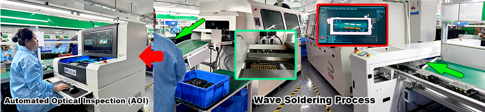
Automated Optical Inspection—commonly known as AOI—is an image-based inspection technology used throughout electronics manufacturing.
Instead of measuring electrical performance, AOI evaluates the physical quality of PCB assemblies.
During inspection, high-resolution cameras capture detailed images of every assembled circuit board.
Specialized software compares these images with predefined reference data.
If the system detects any abnormalities, it immediately alerts operators for further review.
Unlike manual inspection, AOI performs the same evaluation repeatedly without becoming fatigued, making it especially valuable for high-volume production.
Why USB-C Chargers Require High-Precision PCB Inspection
Fast chargers are becoming increasingly compact while delivering significantly higher power.
This combination creates new manufacturing challenges.
Modern USB-C PD and GaN chargers often include:
• Fine-pitch integrated circuits
• High-density PCB layouts
• Miniature passive components
• Multiple power stages
• High-frequency switching circuits
As component density increases, assembly tolerances become tighter.
Even a slight placement error may affect electrical performance.
Although later production stages such as functional testing can identify many problems, discovering defects earlier reduces manufacturing costs and improves process efficiency.
AOI therefore serves as an important checkpoint before products continue through the rest of the production line.
Where AOI Fits Into the Manufacturing Process
Professional charger factories rarely depend on a single inspection method.
Instead, quality verification is distributed throughout production.
A simplified manufacturing sequence may include:
1. SMT solder paste printing
2. Component placement
3. Reflow soldering
4. AOI inspection
5. Manual verification of flagged boards
6. Through-hole assembly (if required)
7. ICT testing
8. Functional testing
9. Hi-Pot testing
10. Aging test
11. Final inspection
12. Packaging
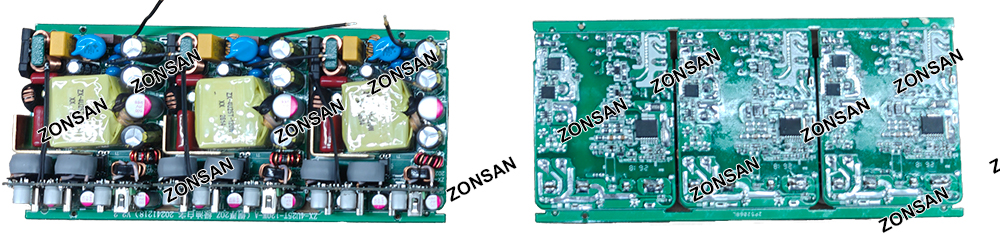
By placing AOI immediately after reflow soldering, manufacturers can identify many assembly defects before additional production resources are invested.
This improves overall manufacturing efficiency while reducing unnecessary downstream failures.
What Can AOI Detect?
Although different AOI systems offer different capabilities, modern equipment is typically able to identify a wide range of assembly defects.
Among the most common are:
Missing Components
If a resistor, capacitor or IC is absent from the PCB, AOI immediately compares the image with the reference design and identifies the missing location.
Incorrect Component Placement
A component may be present but shifted slightly outside its acceptable tolerance.
AOI measures placement accuracy and highlights excessive deviation.
Incorrect Component Orientation
Certain electronic components—including diodes, ICs and polarized capacitors—must be installed with the correct orientation.
Incorrect orientation can prevent normal operation or even damage the circuit.
AOI identifies these installation errors before electrical testing begins.
Solder Joint Defects
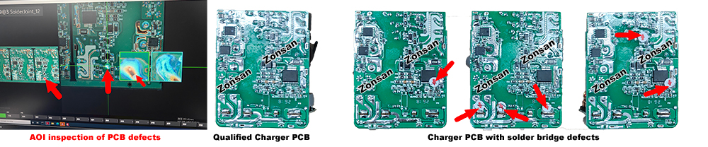
One of AOI's most valuable functions is evaluating solder quality.
Typical issues include:
• Insufficient solder
• Excess solder
• Solder bridges
• Poor wetting
• Open solder joints
Detecting these problems early significantly reduces the likelihood of intermittent failures reaching later production stages.
Professional charger factories rarely depend on a single inspection method.
Instead, quality verification is distributed throughout production.
A simplified manufacturing sequence may include:
1. SMT solder paste printing
2. Component placement
3. Reflow soldering
4. AOI inspection
5. Manual verification of flagged boards
6. Through-hole assembly (if required)
7. ICT testing
8. Functional testing
9. Hi-Pot testing
10. Aging test
11. Final inspection
12. Packaging
By placing AOI immediately after reflow soldering, manufacturers can identify many assembly defects before additional production resources are invested.
This improves overall manufacturing efficiency while reducing unnecessary downstream failures.
What Can AOI Detect?
Although different AOI systems offer different capabilities, modern equipment is typically able to identify a wide range of assembly defects.
Among the most common are:
Missing Components
If a resistor, capacitor or IC is absent from the PCB, AOI immediately compares the image with the reference design and identifies the missing location.
Incorrect Component Placement
A component may be present but shifted slightly outside its acceptable tolerance.
AOI measures placement accuracy and highlights excessive deviation.
Incorrect Component Orientation
Certain electronic components—including diodes, ICs and polarized capacitors—must be installed with the correct orientation.
Incorrect orientation can prevent normal operation or even damage the circuit.
AOI identifies these installation errors before electrical testing begins.
Solder Joint Defects
One of AOI's most valuable functions is evaluating solder quality.
Typical issues include:
• Insufficient solder
• Excess solder
• Solder bridges
• Poor wetting
• Open solder joints
Detecting these problems early significantly reduces the likelihood of intermittent failures reaching later production stages.
Why AOI Is More Than Just Defect Detection
One common misconception is that AOI simply finds defective products.
In reality, experienced manufacturers use AOI as a process improvement tool.
Because every inspection result is recorded digitally, engineering teams can analyze production trends over time.
For example:
• Are solder bridges increasing on one SMT line?
• Does one component feeder show higher placement variation?
• Is a specific PCB design generating repeated inspection alerts?
Answering these questions allows engineers to improve manufacturing processes before defect rates increase.
Instead of only identifying bad products, AOI also helps improve future production quality.
Can AOI Make Mistakes? Understanding False Calls in Automated Inspection
One of the biggest misconceptions about Automated Optical Inspection is that it is always correct.
In reality, even the most advanced AOI systems occasionally identify a good PCB as defective. In manufacturing, these are known as false calls or false positives.
This doesn't mean the machine is unreliable.
Instead, it reflects how sensitive modern inspection systems have become.
AOI compares every solder joint and every component against predefined reference criteria. If lighting conditions, solder reflections, component color variations or acceptable manufacturing tolerances differ slightly from the reference image, the system may flag the board for review.
For this reason, professional manufacturers do not allow AOI to make final quality decisions independently.
Instead, AOI works together with trained quality engineers.
When a board is flagged, inspectors review the image and determine whether it represents:
• A genuine manufacturing defect
• A cosmetic variation within specification
• A false call caused by image interpretation
This combination of automated inspection and human verification helps maintain both efficiency and accuracy.
AOI vs Manual Visual Inspection
Before AOI became widely available, PCB inspection relied almost entirely on experienced operators.
Although manual inspection is still valuable, it has natural limitations.
Human inspectors can become fatigued after examining hundreds or thousands of circuit boards.
Lighting conditions, concentration and individual experience may also influence inspection consistency.
AOI addresses these challenges by performing every inspection according to the same programmed criteria.
The comparison below illustrates the strengths of each method.
| Manual Inspection | AOI Inspection |
| Experience-dependent | Rule-based and consistent |
| May miss very small defects | Detects microscopic placement and solder issues |
| Inspection speed varies | High-speed automated inspection |
| Subject to fatigue | Consistent across long production runs |
| Useful for engineering judgement | Excellent for repetitive inspection tasks |
Professional factories therefore use both methods rather than choosing one over the other.
AOI performs rapid, repeatable screening, while trained engineers investigate complex or unusual cases.
AOI vs ICT: Different Tests for Different Purposes
Another common misunderstanding is that AOI and In-Circuit Testing (ICT) perform the same job.
They do not.
AOI examines what the PCB looks like.
ICT evaluates how the PCB behaves electrically.
For example:
AOI can detect:
• Missing resistors
• Crooked ICs
• Poor solder joints
• Component orientation errors
ICT can detect:
• Open circuits
• Short circuits
• Incorrect resistance values
• Electrical connectivity problems
• Certain component failures that are visually undetectable
Because these inspections complement each other, most professional charger manufacturers use both during production.
Why AOI Cannot Replace Functional Testing
Even if every PCB passes AOI inspection, the finished charger still requires additional verification.
Why?
Because appearance alone cannot confirm product performance.
Consider several examples.
A PCB may be assembled perfectly but contain an internally defective integrated circuit.
A USB Power Delivery controller may negotiate voltage incorrectly due to firmware configuration.
A protection circuit may not activate under overload conditions.
None of these issues can be identified through image inspection alone.
This is why AOI forms only one part of a complete quality assurance system.
Functional testing, Hi-Pot testing and aging tests remain essential before shipment.
AOI performs rapid, repeatable screening, while trained engineers investigate complex or unusual cases.
AOI vs ICT: Different Tests for Different Purposes
Another common misunderstanding is that AOI and In-Circuit Testing (ICT) perform the same job.
They do not.
AOI examines what the PCB looks like.
ICT evaluates how the PCB behaves electrically.
For example:
AOI can detect:
• Missing resistors
• Crooked ICs
• Poor solder joints
• Component orientation errors
ICT can detect:
• Open circuits
• Short circuits
• Incorrect resistance values
• Electrical connectivity problems
• Certain component failures that are visually undetectable
Because these inspections complement each other, most professional charger manufacturers use both during production.
Why AOI Cannot Replace Functional Testing
Even if every PCB passes AOI inspection, the finished charger still requires additional verification.
Why?
Because appearance alone cannot confirm product performance.
Consider several examples.
A PCB may be assembled perfectly but contain an internally defective integrated circuit.
A USB Power Delivery controller may negotiate voltage incorrectly due to firmware configuration.
A protection circuit may not activate under overload conditions.
None of these issues can be identified through image inspection alone.
This is why AOI forms only one part of a complete quality assurance system.
Functional testing, Hi-Pot testing and aging tests remain essential before shipment.

How AOI Data Supports Continuous Manufacturing Improvement
One of the greatest advantages of digital inspection is the amount of process data it generates.
Every inspected PCB contributes valuable information.
Over time, manufacturers can analyze trends such as:
• Which SMT line produces the lowest defect rate?
• Are solder bridge defects increasing during certain production shifts?
• Does a newly introduced component supplier affect placement accuracy?
• Has a process adjustment reduced recurring defects?
Rather than reacting only when failures occur, engineers use AOI data to improve manufacturing proactively.
This data-driven approach supports continuous improvement, reduces variation and helps maintain consistent product quality across large production volumes.
Common Misconceptions About AOI
Even experienced buyers sometimes misunderstand what AOI can and cannot do.
Misconception 1: AOI Guarantees a Perfect Product
No inspection method can eliminate every possible defect.
AOI significantly improves manufacturing quality, but it works alongside ICT, functional testing, aging tests and other quality control processes.
Misconception 2: AOI Can Detect Every Electrical Problem
AOI evaluates physical assembly.
Electrical faults such as incorrect firmware, damaged semiconductors or unstable communication protocols require electrical testing.
Misconception 3: AOI Replaces Skilled Quality Engineers
Automation increases inspection efficiency, but experienced engineers remain essential.
They interpret complex inspection results, investigate root causes and optimize manufacturing processes based on AOI data.
Misconception 4: Only High-End Factories Need AOI
As USB-C chargers become more compact and component density increases, automated inspection has become increasingly important across modern electronics manufacturing.
For products requiring high consistency and international quality standards, AOI is now considered a core element of professional production.
Why AOI Reflects a Manufacturer's Commitment to Quality
For OEM customers evaluating potential suppliers, the presence of AOI equipment alone is not the most important factor.
What matters is how inspection data is used.
Leading manufacturers treat AOI as more than an automated checkpoint.
Inspection results become part of a broader quality management system that includes:
• Root cause analysis
• Corrective and preventive actions (CAPA)
• Process optimization
• Equipment maintenance
• Operator training
• Supplier quality evaluation
This integrated approach allows quality improvements to extend beyond individual products and strengthen the entire manufacturing process.
When used effectively, AOI contributes not only to detecting today's defects but also to preventing tomorrow's.
Final Thoughts
As USB-C chargers continue to evolve, manufacturing precision becomes increasingly important.
Smaller components, higher power densities and more sophisticated circuit designs leave less room for assembly variation.
Automated Optical Inspection helps manufacturers maintain consistent PCB quality by identifying assembly defects before they progress further down the production line.
More importantly, AOI represents a shift from reactive quality control to proactive manufacturing improvement.
By combining advanced inspection technology with experienced engineering teams, professional charger factories can improve efficiency, reduce hidden defects and deliver more reliable products to customers around the world.
For OEM and ODM buyers, understanding how a manufacturer integrates AOI into its production process offers valuable insight into its overall commitment to quality, consistency and continuous improvement.
Frequently Asked Questions (FAQ)
Q1: What is AOI in charger manufacturing?
AOI (Automated Optical Inspection) uses cameras and image analysis software to inspect PCB assemblies for manufacturing defects after SMT assembly.
Q2: What kinds of defects can AOI detect?
AOI can detect missing components, incorrect placement, incorrect orientation, solder bridges, insufficient solder, open solder joints and other visible assembly defects.
Q3: Can AOI detect electrical faults?
Not directly. AOI evaluates physical assembly quality, while electrical faults are identified through tests such as ICT and functional testing.
Q4: Why do manufacturers perform AOI before functional testing?
Detecting assembly defects early reduces rework, improves production efficiency and prevents defective boards from moving further through the manufacturing process.
Q5: What is a false call in AOI?
A false call occurs when the AOI system flags a correctly assembled PCB as defective due to image interpretation or acceptable manufacturing variation. Engineers review these cases manually.
Q6: Does AOI replace manual inspection?
No. Professional manufacturers combine AOI with experienced quality engineers to achieve both efficiency and accurate decision-making.
Q7: Why is AOI important for USB-C GaN chargers?
High-density PCB layouts and miniature components require highly consistent inspection that is difficult to achieve through manual methods alone.
Q8: How does AOI improve long-term manufacturing quality?
By collecting inspection data, AOI helps engineers identify process trends, optimize production and reduce recurring defects over time.
Recommended
• Environmental Testing for USB-C Power Adapters: How Professional Manufacturers Verify Reliability in Real-World Conditions.↗
• Understanding Hi-Pot Testing for USB-C Chargers: How Professional Manufacturers Verify Electrical Safety Before Shipment.↗
• How PCB Layout Determines Charger Performance: Inside the Engineering Behind Fast Chargers.↗