How PCB Layout Determines Charger Performance: Inside the Engineering Behind Fast Chargers
Quick Answer (Featured Snippet)
PCB layout is one of the most critical factors in charger design. A well-designed PCB improves power efficiency, reduces heat generation, minimizes electromagnetic interference (EMI), enhances charging stability, and increases long-term reliability. Even when two chargers use the same electronic components, different PCB layouts can result in significantly different performance, safety, and lifespan.
Key Takeaways
PCB layout affects almost every aspect of charger performance.
Electrical current paths determine efficiency and heat generation.
Proper component placement helps reduce EMI and improve reliability.
High-power GaN chargers require more sophisticated PCB design than conventional chargers.
Professional charger manufacturers spend weeks reviewing PCB layouts before mass production.
Introduction
When people think about a fast charger, they usually focus on visible specifications such as power output, charging protocols, or the number of USB ports. It's easy to compare a 65W charger with a 100W charger, or choose between GaN and traditional silicon technology.
What rarely gets attention is the green circuit board hidden inside the charger.
To most users, it looks like nothing more than a platform for mounting electronic components.
To an engineer, however, the printed circuit board—or PCB—is where the entire charger comes to life.
The PCB is far more than a support structure. It determines how electricity flows, how heat spreads, how efficiently energy is converted, and even whether the charger can pass EMC certification. A poorly designed PCB can turn premium electronic components into an unreliable product, while an optimized layout allows the same components to perform safely and efficiently for years.
This is why experienced charger engineers often say:
"A charger is only as good as its PCB layout."
Understanding PCB design doesn't require an engineering degree, but it does help explain why two chargers with nearly identical specifications can deliver completely different real-world performance.
Why PCB Layout Matters More Than Most People Realize
Every fast charger contains dozens of electronic components.
These may include:
• Power controller IC
• GaN transistors or MOSFETs
• Transformer
• Capacitors
• Inductors
• USB-C PD controller
• Protection ICs
• Feedback circuits
• EMI filters
Many people assume that component quality alone determines charger performance.
In reality, components are only part of the equation.
Imagine placing all the parts of a high-performance sports car into a garage without connecting them properly. Even the world's best engine cannot deliver performance if every part is positioned incorrectly.
A PCB works in much the same way.
It provides the electrical pathways that connect every component into one complete power conversion system.
If those pathways are too long, poorly positioned or improperly routed, problems begin to appear:
• Higher electrical resistance
• Increased heat
• Greater switching noise
• Reduced efficiency
• Poor voltage stability
• More difficult EMC compliance
Good PCB layout prevents these issues before the first prototype is even assembled.
Following the Path of Electricity
One helpful way to understand PCB design is to follow the journey of electricity through a charger.
After AC power enters the charger, it doesn't immediately reach your phone or laptop.
Instead, it passes through a carefully designed sequence of circuits.
A simplified flow looks like this:
AC Input
↓
EMI Filter
↓
Bridge Rectifier
↓
Primary Switching Circuit
↓
High-Frequency Transformer
↓
Secondary Rectification
↓
Output Filter
↓
USB-C Power Delivery Controller
↓
Connected Device
Each section performs a different task, and the PCB determines how efficiently these sections communicate with one another.
If one stage is poorly arranged, the effects can spread throughout the entire charger.
For example, increasing the distance between the transformer and output rectifier may appear insignificant on paper. Yet it can increase conduction losses, raise operating temperatures and reduce overall efficiency.
These are the kinds of details engineers spend countless hours refining.

How PCB Layout Influences Charging Efficiency
Efficiency is often advertised as a percentage.
A charger may claim 92%, 94% or even higher conversion efficiency.
Many users assume that this figure depends entirely on the semiconductor devices inside the charger.
While component selection certainly matters, PCB layout plays an equally important role.
Electricity naturally follows the path of least resistance.
Every additional millimeter of copper trace adds resistance, however small it may seem.
Longer current paths create:
• Additional voltage drop
• Higher power loss
• More heat generation
• Reduced conversion efficiency
Engineers therefore aim to keep high-current paths as short and direct as possible.
This is especially important in high-power USB-C chargers where output currents can reach 5A or more.
At these current levels, seemingly minor layout improvements can noticeably improve efficiency.
Copper thickness also contributes to performance.
Thicker copper reduces resistance and improves heat dissipation, but it also increases manufacturing cost.
Engineering is therefore a balance between electrical performance, thermal requirements and commercial practicality.
Heat Begins with Layout
Heat management is one of the biggest engineering challenges in modern fast chargers.
Contrary to popular belief, overheating is not always caused by poor-quality components.
Sometimes the issue begins with PCB layout.
When power devices are placed too close together, heat accumulates in a confined area.
This creates local hotspots that may not be obvious during initial testing but become increasingly problematic during prolonged full-load operation.
Professional engineers therefore pay close attention to component placement.
High-power devices are arranged to:
• Improve airflow inside the enclosure
• Reduce thermal interaction between components
• Spread heat across larger copper areas
• Transfer heat efficiently to thermal pads or the housing
Even moving one component by only a few millimeters can lower operating temperatures by several degrees.
Although these adjustments sound small, they have a measurable impact on product lifespan.
Electrolytic capacitors, for example, are particularly sensitive to heat.
Reducing their operating temperature by just a few degrees can significantly extend service life.
Why PCB Layout Determines EMI Performance
One of the least visible—but most important—aspects of charger engineering is electromagnetic compatibility, commonly known as EMC.
Every switching power supply generates high-frequency electrical noise.
If this noise is not properly controlled, it can interfere with nearby electronic devices, wireless communication or even prevent the charger from passing regulatory certification.
Interestingly, many EMC issues originate not from faulty components but from PCB layout itself.
For example, engineers carefully control the size of high-frequency switching loops.
A larger switching loop acts like an antenna, radiating unwanted electromagnetic energy into the surrounding environment.
Reducing loop area helps minimise this radiation before additional filtering is even required.
Grounding strategy is equally important.
Rather than treating the ground plane as a simple copper layer, engineers use it as a carefully planned reference system that stabilises signals, reduces electrical noise and improves overall circuit behaviour.
Effective EMI design is therefore not something added at the end of development.
It begins with the very first PCB layout.
Component Placement Is Never Random
Looking at the inside of a charger, some people assume components are arranged simply to fit inside a compact enclosure.
In reality, every placement decision is intentional.
For example:
• High-voltage circuits are separated from low-voltage output sections.
• Sensitive control ICs are positioned away from noisy switching components.
• Thermal-sensitive capacitors are kept away from major heat sources.
• High-current paths are shortened to minimise electrical losses.
• USB-C controller circuits are located to maintain stable signal integrity.
These design principles work together to improve efficiency, reliability and manufacturability.
Poor placement may still produce a functioning prototype, but long-term performance is often compromised.
Professional engineering teams therefore spend considerable time reviewing layouts before authorising prototype production.
Two Chargers Can Share the Same Components — Yet Perform Very Differently
One misconception in the market is that comparing component lists tells the whole story.
Suppose two manufacturers purchase the same controller IC, transformer, GaN devices and capacitors.
On paper, the bill of materials appears almost identical.
Yet one charger consistently operates cooler, passes EMC testing with fewer revisions and demonstrates higher long-term reliability.
Why?
Often, the difference lies in PCB engineering.
Optimised routing, balanced thermal distribution, proper grounding and careful component placement allow each component to perform closer to its intended capability.
In contrast, a less refined layout may force those same components to operate under greater electrical and thermal stress.
This is why experienced OEM buyers increasingly ask not only about the components used, but also about the engineering process behind the PCB design.
Common PCB Layout Mistakes That Affect Charger Performance
Even experienced engineers rarely complete a PCB layout perfectly on the first attempt. Modern USB-C chargers integrate high-frequency switching circuits, power conversion stages, communication protocols, and multiple protection systems into a very limited space. Small layout issues that seem insignificant during design can become major problems during prototype testing.
Below are several common PCB layout mistakes seen in charger development.
1. Excessively Long High-Current Traces
High-current output paths should always be kept as short and direct as possible.
When these traces become unnecessarily long, electrical resistance increases. The result is greater power loss, higher operating temperatures and lower conversion efficiency.
In high-power 100W or 140W chargers, this issue becomes even more noticeable because output currents can exceed 5A under USB PD 3.1 Extended Power Range (EPR).
2. Poor Separation Between High-Voltage and Low-Voltage Areas
Inside every charger, the primary side handles high AC voltage while the secondary side delivers low-voltage DC power to connected devices.
If these two areas are positioned too closely or the isolation spacing is insufficient, the charger may fail international safety requirements such as IEC 62368-1 or experience increased electrical interference.
Maintaining proper creepage and clearance distances is therefore a fundamental part of PCB design rather than a simple manufacturing rule.
3. Concentrating Heat-Generating Components
Another frequent mistake is placing the transformer, GaN devices, synchronous rectifiers and electrolytic capacitors too close together.
While this may save space, it often creates localized hot spots that shorten component lifespan.
A better approach distributes heat sources more evenly and allows thermal energy to spread through larger copper areas before reaching temperature-sensitive components.
4. Inadequate Ground Plane Design
A fragmented or poorly planned ground plane can introduce signal instability, increase switching noise and complicate EMC compliance.
Professional engineers usually treat the ground plane as an active part of the electrical design rather than simply filling unused PCB space with copper.
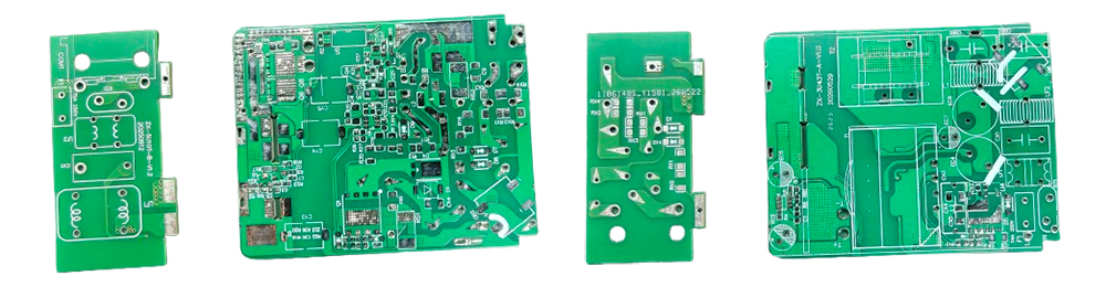
Why High-Power GaN Chargers Often Use Multi-Layer PCBs
As charging power increases, PCB complexity increases as well.
Many compact smartphone chargers delivering 20W or 30W can perform well using a two-layer PCB because current levels remain relatively low and routing requirements are straightforward.
However, once output power reaches 65W, 100W or even 140W, the design requirements change significantly.
Higher-power chargers often benefit from four-layer PCB construction because additional layers provide several engineering advantages.
They allow engineers to:
• Reduce electrical resistance through improved power distribution.
• Create continuous ground planes that suppress electromagnetic interference.
• Separate high-speed control signals from noisy switching circuits.
• Improve heat spreading across larger copper areas.
• Simplify complex routing without compromising safety spacing.
This doesn't mean every high-power charger must use four layers. Product size, topology, cost targets and thermal requirements all influence the final decision.
The important point is that PCB layer count is an engineering choice—not simply a manufacturing specification.
PCB Layout Review: One of the Most Important Engineering Stages
Before a prototype is manufactured, professional engineering teams spend significant time reviewing the PCB layout.
The objective is simple:
Find potential problems before they become expensive hardware revisions.
A typical review covers questions such as:
• Are high-current paths sufficiently short?
• Are sensitive control circuits isolated from switching noise?
• Does the transformer have adequate clearance?
• Are thermal hotspots likely to develop?
• Is the USB-C controller positioned appropriately?
• Can the design meet EMC requirements?
• Does the layout support efficient manufacturing?
Many design improvements happen during this stage, long before the first PCB is produced.
Experienced teams know that correcting a layout in software takes minutes, while redesigning physical prototypes after testing may delay an entire project by weeks.
How Professional Charger Manufacturers Optimize PCB Layout
For professional charger manufacturers, PCB layout is not handled by a single engineer working independently.
Instead, it is a collaborative engineering process.
For example, during the development of a new GaN charger, hardware engineers may optimize the power stage, while EMC engineers evaluate switching noise, thermal engineers analyze heat distribution, and manufacturing engineers review whether the design can be produced consistently on automated SMT lines.
Each review adds another layer of refinement.
At ZONSAN, PCB layouts are evaluated alongside schematic verification, thermal analysis, manufacturability assessment and reliability planning before entering prototype production.
This cross-functional approach helps reduce development risk and increases the likelihood of achieving stable performance, successful certification and smooth mass production.

Final Thoughts
When people compare chargers, they often focus on visible specifications such as charging power, USB ports or supported protocols.
These specifications certainly matter, but they represent only part of the engineering story.
Much of a charger's real performance is determined by decisions that users never see.
PCB layout influences how efficiently power flows, how effectively heat is managed, how well electromagnetic interference is controlled and how reliably the product performs after years of everyday use.
Two chargers may advertise identical specifications and even use similar components, yet thoughtful PCB engineering can make one noticeably cooler, quieter and more reliable than the other.
For OEM buyers evaluating charger manufacturers, understanding the importance of PCB design provides valuable insight into the engineering capabilities behind the finished product.
Ultimately, excellent chargers are not defined solely by the components they contain—they are defined by how intelligently those components work together.
Frequently Asked Questions (FAQ)
Q1: Why is PCB layout so important in a charger?
Because it directly affects efficiency, heat generation, EMI performance, charging stability and long-term reliability.
Q2: Can two chargers use the same components but perform differently?
Yes. PCB layout, thermal design and manufacturing quality can produce significant performance differences even when component lists are similar.
Q3: Do GaN chargers require different PCB layouts?
Generally, yes. Higher switching frequencies and compact designs require more careful routing, grounding and thermal management.
Q4: Does PCB thickness affect charger performance?
Copper thickness and board construction can influence current carrying capability, thermal performance and voltage loss.
Q5: Why are high-current traces kept short?
Shorter traces reduce electrical resistance, improve efficiency and generate less heat.
Q6: What is the purpose of the ground plane?
A properly designed ground plane improves signal stability, reduces electrical noise and helps achieve EMC compliance.
Q7: Why do some fast chargers use four-layer PCBs?
Four-layer boards provide better routing flexibility, lower EMI and improved thermal performance for high-power applications.
Q8: How do charger manufacturers verify PCB quality before production?
Through schematic reviews, PCB layout reviews, prototype validation, thermal testing, EMC testing and manufacturing assessments.
More articles about charger factory production
• How a USB-C Charger Is Designed: From Circuit Concept to Mass Production.↗
• Inside a Charger: PCB, IC and Transformer Explained.↗
• How Charger Safety Certifications Prove Product Quality.↗
Recommended reading on charger PCB information
• IPC PCB Design Standards.↗
• Texas Instruments – PCB Layout Guidelines.↗