How a USB-C Charger Is Designed: From Circuit Concept to Mass Production
Quick Answer (Featured Snippet)
Designing a modern USB-C charger involves far more than selecting a power rating. Professional charger manufacturers begin with product requirements, then develop the power architecture, schematic, transformer, PCB layout, thermal management, USB Power Delivery firmware, safety protection and manufacturing process before validating the design through engineering tests and mass production. Every stage influences charging efficiency, safety, reliability and certification success.
Why Good Chargers Are Designed, Not Assembled
To many consumers, a charger looks like a simple accessory.
Plug it into the wall.
Connect a USB-C cable.
The battery starts charging.
Simple.
From an engineer's perspective, however, a charger is one of the most compact and demanding power conversion systems in modern consumer electronics.
Inside a charger smaller than the palm of your hand, engineers must solve several competing challenges at the same time.
The charger must deliver stable power while remaining compact, efficient and cool. It must support multiple charging protocols, withstand years of daily use, comply with international safety standards and remain economical to manufacture at scale.
Every millimeter of internal space matters.
Every electronic component influences another.
Every engineering decision affects the final product.
This is why professional charger design is never about assembling random electronic parts.
It is about building a complete power conversion system where every subsystem works together.
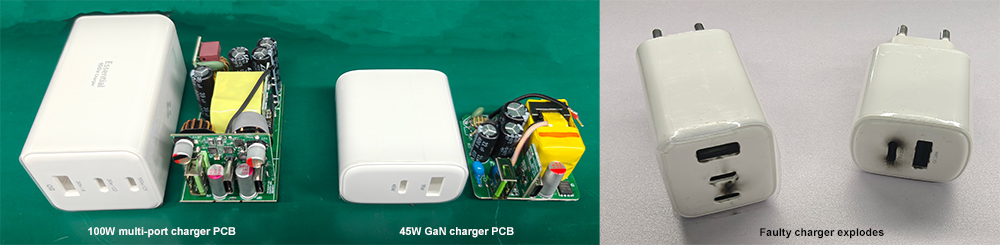
Every Successful Charger Starts With a Question
Before engineers open schematic software or begin PCB layout, they ask one simple question: What problem is this charger designed to solve?
Different products require completely different engineering priorities.
Consider these examples:
A 20W USB-C charger is optimized for smartphones and compact size.
A 45W PPS charger must negotiate voltage dynamically with Samsung Galaxy devices.
A 65W GaN charger balances high efficiency with reduced dimensions.
A 100W desktop charger must manage multiple ports while maintaining stable power distribution.
A 140W PD3.1 charger introduces Extended Power Range (EPR) requirements, placing greater demands on thermal design, transformer performance and USB Power Delivery communication.
Although all of these products are "chargers," they are fundamentally different engineering projects.
Step 1 — Defining Product Requirements
Every development project begins with a specification document.
This document answers questions such as:
• What devices will the charger support?
• What charging protocols are required?
• What power output is expected?
• Which countries will the product be sold in?
• What certifications will be required?
• What physical size limitations exist?
• What cost target must be achieved?
Only after these requirements are clearly defined can engineering work begin.
Changing fundamental requirements halfway through development often increases both cost and development time.
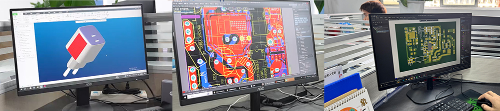
Step 2 — Choosing the Power Architecture
Once product requirements are established, engineers determine how electrical energy will flow through the charger.
This is known as the power architecture.
Although every design differs, a typical USB-C GaN charger contains several functional stages:
AC Input
↓
EMI Filter
↓
Bridge Rectifier
↓
Primary Switching Circuit
↓
High-Frequency Transformer
↓
Secondary Rectification
↓
Output Filtering
↓
USB-C PD Controller
↓
Device Communication
Each stage performs a unique function.
Improving one stage often influences another.
For example, increasing switching frequency can reduce transformer size but may increase electromagnetic interference.
Improving efficiency can reduce heat but may increase component cost.
Engineering is always a balance between performance, manufacturability and reliability.
Why Modern Chargers Are More Complex Than Ever
Older USB chargers typically delivered a fixed 5V output.
Today's chargers are dramatically more intelligent.
A modern USB-C PD charger must communicate with the connected device before delivering higher voltages.
During just a few milliseconds, the charger determines:
• Device capability
• Cable capability
• Supported charging protocol
• Requested voltage
• Requested current
• Maximum available power
Only after successful negotiation does high-power charging begin.
This communication process is one reason why modern charger development requires expertise in both hardware and embedded firmware.
Engineer's Insight
One of the most common misconceptions is that designing a 100W charger is simply a matter of using larger components than a 20W charger.
In reality, increasing power fundamentally changes the engineering challenge.
Higher power affects transformer design, thermal management, PCB layout, protection strategies, EMI performance and manufacturing tolerances.
As power levels increase, the interactions between these systems become increasingly complex.
For experienced charger engineers, the real challenge is not delivering more power—it's doing so safely, efficiently and consistently over years of operation.
From Components to Circuit: Building the Core of a USB-C Charger
Step 3 — Selecting the Right Electronic Components
Once the overall power architecture has been defined, engineers begin selecting the components that will determine how the charger performs in the real world.
At first glance, two 65W USB-C chargers may appear almost identical. They both support USB Power Delivery, both charge a laptop at the same speed, and both meet the same output specification.
Internally, however, they can be completely different products.
The difference lies in component selection.
Every resistor, capacitor, transformer and power device contributes to the charger's efficiency, thermal behavior, electromagnetic compatibility and long-term reliability.
Professional charger design is therefore less about finding the cheapest component and more about choosing components that work together as a complete power system.
Controller IC
The controller IC acts as the brain of the power supply.
It regulates switching frequency, monitors feedback signals and adjusts output according to changing load conditions.
Modern USB-C PD chargers also require communication with USB-C controllers to negotiate voltage and current with connected devices.
An unstable controller can affect:
• Output regulation
• Efficiency
• Thermal performance
• Protection timing
• USB-C negotiation stability
GaN Devices vs Silicon MOSFETs
One of the biggest advances in charger development over the past decade has been the adoption of Gallium Nitride (GaN) devices.
Compared with traditional silicon MOSFETs, GaN devices switch much faster while generating lower switching losses.
This allows engineers to:
• Increase switching frequency
• Reduce transformer size
• Improve efficiency
• Lower operating temperature
• Build smaller chargers
However, GaN also requires more precise PCB layout and thermal management.
Higher switching speeds leave less room for design errors, making engineering expertise even more important.
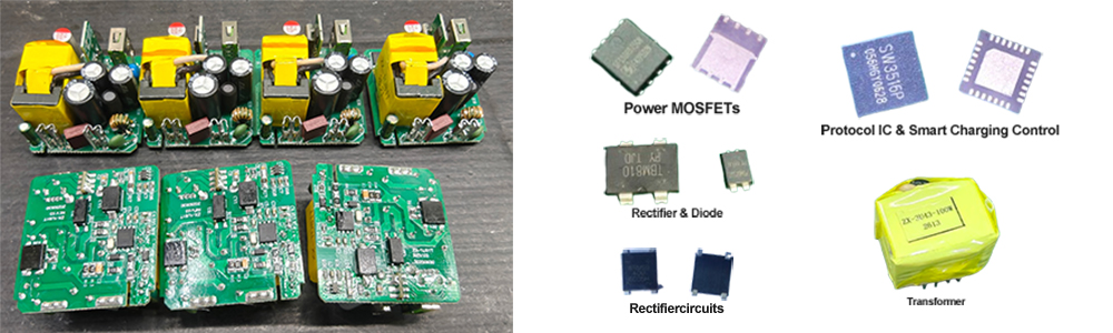
Capacitors
Consumers rarely think about capacitors, yet they are among the most important components inside any charger.
They smooth voltage, reduce ripple and stabilize the power supply.
Higher-quality capacitors generally offer:
• Better heat resistance
• Longer service life
• Lower ESR
• Improved reliability under continuous operation
Selecting capacitors is always a balance between electrical performance, available space and product lifespan.
Engineering Decision
Why Don't Engineers Simply Choose the Highest-Spec Components?
A common misconception is that better chargers are built by selecting the most expensive components available.
In reality, engineering is an exercise in optimization.
Using an oversized transformer may improve thermal performance but increase cost and reduce available PCB space.
Selecting an ultra-fast switching device may improve efficiency but create additional EMI challenges.
Every decision affects multiple aspects of the design.
The goal is not to maximize one specification.
The goal is to optimize the entire system.
Reding:Inside a Charger: PCB, IC, Transformer Explained.↗
Step 4 — Why the Transformer Is the Heart of Every Charger
Ask experienced charger engineers which component has the greatest influence on overall performance, and many will give the same answer:
The transformer.
Unlike traditional low-frequency transformers used in older power supplies, modern USB-C chargers use high-frequency transformers operating at tens or even hundreds of kilohertz.
These transformers provide:
• Electrical isolation
• Voltage conversion
• Power transfer
• Safety separation between input and output
Designing a transformer is a highly specialized engineering task.
Engineers must calculate:
• Core material
• Turns ratio
• Wire diameter
• Winding arrangement
• Leakage inductance
• Copper loss
• Core loss
• Temperature rise
Even small adjustments can significantly affect efficiency and thermal performance.
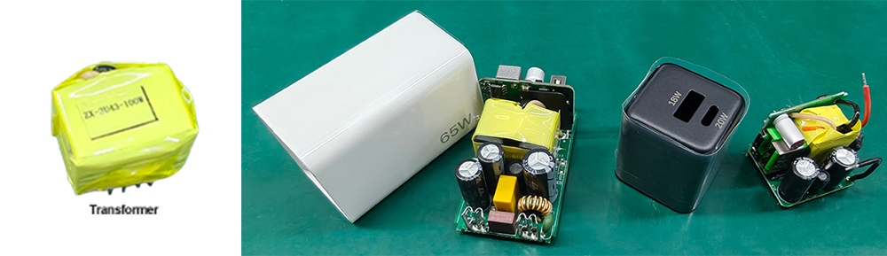
Why Transformer Design Influences Charger Size
Modern GaN chargers are often praised for being remarkably compact.
While GaN devices receive most of the attention, transformer optimization plays an equally important role.
Higher switching frequencies allow engineers to reduce transformer dimensions without sacrificing output power.
However, reducing size also makes heat management more challenging.
This is why compact charger design is always a compromise between efficiency, power density and thermal stability.
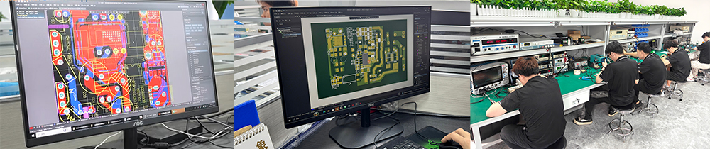
Step 5 — PCB Layout: Where Good Designs Become Great Products
If the schematic defines how a charger should work, the PCB layout determines how well it actually works.
A poorly designed PCB can cause:
• Excessive heat
• Electromagnetic interference
• Unstable output
• Failed certification
• Reduced efficiency
Conversely, a well-designed PCB improves performance without changing a single component.
Professional PCB layout requires careful attention to:
• High-current paths
• Switching loops
• Ground planes
• Creepage distances
• Clearance distances
• Component spacing
• Thermal distribution
Engineers often spend as much time refining PCB layout as they do creating the original circuit.
Engineering Decision
Why Doesn't a 100W Charger Simply Use a Larger Version of a 20W PCB?
Higher power fundamentally changes electrical behavior.
As current increases, engineers must consider:
• Wider copper traces
• Lower resistance paths
• Improved thermal spreading
• Increased creepage distances
• Better EMI control
This is why high-power chargers often use multi-layer PCBs, while lower-power chargers can achieve good performance with simpler layouts.
The PCB evolves together with the power level—it does not simply scale in size.
Engineer's Insight
One of the most common reasons early prototypes fail is not because the circuit is incorrect, but because the PCB layout doesn't fully support the design.
A schematic can look perfect on paper.
Once switching currents begin flowing through a real PCB, however, parasitic inductance, trace resistance and electromagnetic coupling reveal problems that simulation alone cannot predict.
This is why experienced engineers expect multiple PCB revisions before a charger reaches production readiness.
Engineering Validation: Turning a Charger Design Into a Production-Ready Product
Step 6 — From Prototype to Production: The Engineering Validation Process
A charger design that works in simulation is only the beginning.
Before a USB-C charger enters mass production, professional manufacturers must verify that the design performs reliably under real-world conditions.
This process is usually divided into several engineering validation stages:
• EVT (Engineering Validation Test)
• DVT (Design Validation Test)
• PVT (Production Validation Test)
Each stage answers a different question.
EVT — Engineering Validation Test
Does the design concept actually work?
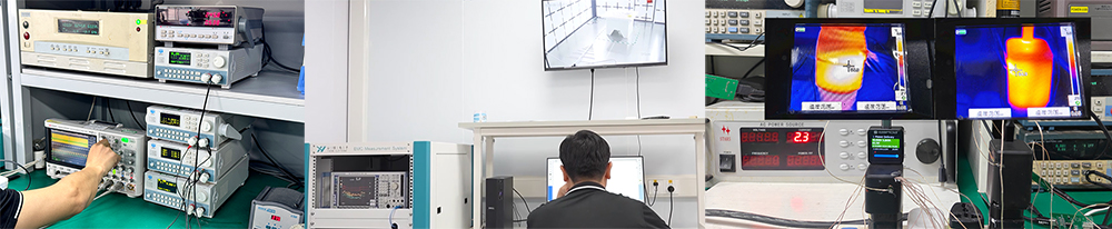
The EVT stage is the first major verification point after prototype development.
At this stage, engineers focus primarily on electrical performance.
The goal is not appearance.
The goal is proving that the core circuit architecture functions correctly.
Typical EVT testing includes:
• Output voltage accuracy
• Power delivery negotiation
• Efficiency measurement
• Protection circuit testing
• Thermal evaluation
• Load testing
• Basic reliability checks
For example, when developing a 100W USB-C PD charger, engineers need to verify:
Can the charger actually deliver 100W continuously?
Does the USB-C PD controller negotiate correctly?
Does the power stage remain stable under maximum load?
Does temperature remain within acceptable limits?
If problems appear during EVT, engineers return to the design stage.
Possible improvements may include:
• Adjusting component values
• Redesigning PCB routing
• Changing thermal solutions
• Optimizing firmware parameters
DVT — Design Validation Test
Does the final design meet all requirements?
After EVT confirms that the basic electrical design works, the product enters DVT.
This stage focuses on complete product validation.
Unlike EVT, DVT evaluates the charger as a finished product.
Testing may include:
Electrical Performance
• Full-load output
• Multi-port power distribution
• Voltage regulation
• Charging protocol compatibility
Safety Performance
• Over-temperature protection
• Short circuit protection
• Over-current protection
• Abnormal operation testing
Mechanical Performance
• Drop testing
• Plug durability
• Housing strength
• Assembly quality
Environmental Testing
• High-temperature operation
• Low-temperature operation
• Humidity testing
At this stage, engineers are asking: "Can this charger survive real customer usage?"
A product that performs well only inside a laboratory is not ready for commercial production.
PVT — Production Validation Test
Can the factory manufacture this charger consistently?
Many people underestimate this stage.
A charger that works perfectly as a prototype does not automatically mean it can be produced thousands or millions of times.
PVT focuses on manufacturing capability.
Engineers verify:
• Production equipment
• Assembly procedures
• Testing stations
• Worker instructions
• Quality checkpoints
• Production yield
For example:
A prototype may be assembled carefully by engineers.
Mass production requires:
• Hundreds of workers
• Automated equipment
• Repeatable processes
• Consistent component placement
The challenge changes from:
"Can we build one good charger?"
to:
"Can we build thousands of identical chargers?"
Engineering Decision
Why Can't Manufacturers Skip EVT or DVT?
Some companies attempt to shorten development cycles by moving directly into production.
This often creates problems later:
• Certification failures
• High return rates
• Thermal issues
• Customer complaints
• Production delays
Professional charger manufacturers understand that early engineering investment reduces long-term cost.
Finding a problem during prototype development may cost hours.
Finding the same problem after mass production may cost thousands of units.
Reding:How Charger Safety Certifications Prove Product Quality.↗
Step 7 — Thermal Engineering: Managing Heat Inside Compact Chargers
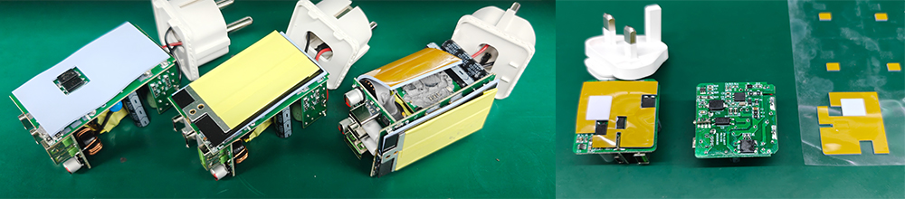
Heat is one of the biggest challenges in modern charger design.
As charging power increases:
20W →
65W →
100W →
140W →
240W
the amount of energy processed inside a small enclosure increases dramatically.
Even highly efficient chargers generate heat.
The engineering challenge is: How can we transfer and control heat before it affects reliability?
Where Does Charger Heat Come From?
Heat mainly comes from: Power Conversion Losses
No power supply reaches 100% efficiency.
During energy conversion, a small amount of electrical energy becomes heat.
Switching Losses
High-frequency switching devices experience losses during:
• Turn-on
• Turn-off
• Voltage transitions
This becomes especially important in high-power GaN chargers.
Component Resistance
Every component has electrical resistance.
Current flowing through resistance generates heat.
This is why:
• PCB copper thickness
• Component selection
• Layout optimization
all matter.
How Engineers Improve Thermal Performance
Professional charger design uses several strategies.
1. Component Placement Optimization
Heat-generating components are positioned carefully.
For example:
• GaN devices
• Transformer
• Rectifiers
must be arranged to prevent heat concentration.
2. Thermal Materials
Engineers may use:
• Thermal pads
• Thermal tapes
• Heat spreaders
• Conductive materials
to transfer heat away from critical components.
3. PCB Thermal Design
The PCB itself can help distribute heat.
Engineers optimize:
• Copper area
• Thermal vias
• Layer structure
to improve heat spreading.
Engineering Decision
Why Smaller Chargers Are Sometimes More Difficult to Design
A larger charger has more internal space.
This allows:
• Larger components
• More airflow
• Easier heat distribution
A compact GaN charger has far less space.
Engineers must solve:
• More power
• Smaller size
• Lower temperature
• Higher efficiency
at the same time.
This is why miniaturized high-power chargers require much more engineering expertise.
Step 8 — EMI Engineering: Why Some Chargers Create Interference
Another major engineering challenge is electromagnetic interference (EMI).
Modern chargers use high-frequency switching technology.
This improves efficiency but also creates electromagnetic noise.
If not properly controlled, EMI can affect:
• Wireless devices
• Communication equipment
• Nearby electronics
and may cause certification failures.
How Engineers Control EMI
EMI performance depends on many design decisions.
Including: PCB Layout
Shorter switching loops reduce unwanted noise.
Filtering Components
Engineers use:
• Common mode chokes, Capacitors, Filters
to suppress interference.
Transformer Design
Transformer structure affects:
• Noise coupling, Leakage, Radiation
Shielding
Some designs require additional shielding solutions.
Engineer's Insight
EMI problems are often discovered late because they are invisible during normal operation.
A charger may:
• Charge devices normally
• Deliver correct power
• Stay within temperature limits
but still fail certification because electromagnetic emissions exceed limits.
This is why experienced engineers consider EMI from the earliest design stage—not after the product is finished.
Step 9 — USB-C PD Firmware: The Intelligence Inside Modern Chargers
Hardware alone cannot create a modern fast charger.
USB-C PD chargers require intelligent communication.
The charger must understand:
• Connected device requirements
• Cable capability
• Supported voltage levels
• Power negotiation rules
This communication is controlled through firmware.
For example:
A 65W PD charger may support:
• 5V / 9V / 12V / 15V / 20V
The charger does not simply output maximum power.
It communicates with the device and provides the requested power profile.
Advanced charging technologies such as:
• PPS, PD3.1, AVS
require even more sophisticated control.
Engineering Decision
Why Firmware Is Becoming More Important in Charger Design
Traditional chargers were mostly hardware products.
Modern USB-C chargers are becoming intelligent power systems.
Future chargers must support:
• More devices
• Higher power levels
• Dynamic voltage adjustment
• Better efficiency
• Smarter protection
This means charger manufacturers increasingly need both:
• Power electronics engineers
• Embedded firmware engineers
Engineer's Insight
The future competition in charger manufacturing will not only be about who can build smaller products.
It will be about who can combine:
• Power electronics
• Semiconductor technology
• Firmware intelligence
• Thermal engineering
• Manufacturing precision
The charger is becoming a smart energy management device rather than a simple power adapter.
From Engineering Design to Mass Production: How Professional USB-C Chargers Are Manufactured
A charger that performs well in the laboratory is only halfway through its journey.
The real challenge begins when engineers ask a different question: Can this design be manufactured consistently, efficiently and reliably at scale?
Designing a charger and manufacturing thousands of identical chargers are two very different engineering disciplines.
A successful OEM charger manufacturer must ensure that every production unit performs like the validated prototype—not just the first engineering sample.
This is where Design for Manufacturing (DFM) becomes essential.
Step 10 — Design for Manufacturing (DFM)
One of the most common reasons products encounter production problems is that they were designed without considering how they would actually be manufactured.
A PCB that looks perfect in CAD software may be difficult to assemble automatically.
A component placed too close to another may increase soldering defects.
A housing with an overly complex internal structure may slow down assembly and reduce production efficiency.
This is why experienced charger manufacturers review every design from a manufacturing perspective before production begins.
The objective of DFM is simple: Design products that are not only functional but also easy to manufacture with consistent quality.
During DFM reviews, engineers evaluate questions such as:
• Can SMT machines accurately place every component?
• Are solder joints accessible for inspection?
• Does the PCB allow efficient heat dissipation?
• Can automated testing equipment easily access test points?
• Will assembly workers have enough space to install internal components without causing damage?
A well-executed DFM process improves product quality while reducing production cost and defect rates.
Engineering Decision
Why Engineers Sometimes Modify a "Good" PCB Before Production
It may seem unnecessary to change a PCB that already functions correctly.
However, engineering is not only about making a product work—it is also about making it manufacturable.
For example:
• Rotating a component by a few degrees may improve automated soldering.
• Increasing the spacing between two components can reduce rework.
• Relocating test pads may speed up functional testing.
These adjustments rarely change electrical performance, but they significantly improve production efficiency and consistency.
Step 11 — SMT: Building the PCB With Precision
Once the design is finalized, production begins with Surface Mount Technology (SMT).
This is where tiny electronic components are mounted onto the printed circuit board with high-speed automated equipment.
Modern SMT production lines can place tens of thousands of components every hour with exceptional accuracy.
The process typically includes:
1. Solder paste printing
2. Automated component placement
3. Reflow soldering
4. Automated Optical Inspection (AOI)
5. Manual verification (if required)
Each stage contributes to the overall quality of the finished charger.

Why SMT Accuracy Matters
A modern 65W or 100W GaN charger contains dozens—sometimes hundreds—of electronic components.
Even a slight deviation in placement can result in:
• Poor solder joints
• Electrical instability
• Reduced reliability
• Increased heat generation
This is why professional factories continuously calibrate SMT equipment and inspect production quality throughout the process.
Automation improves consistency, but engineering oversight remains essential.
Step 12 — Assembly: Turning Components Into a Finished Charger
After the PCB has passed inspection, it moves to the assembly stage.
Here, the electronic module is integrated into the charger housing along with all mechanical components.
Assembly includes:
• Installing insulation materials
• Positioning the transformer
• Securing thermal pads
• Connecting the AC plug assembly
• Fixing the PCB
• Closing the enclosure
• Laser marking or printing certification information
Although these tasks may appear straightforward, assembly quality has a direct impact on product safety.
Improper insulation placement or incorrect screw torque can compromise long-term reliability.

Engineer's Insight
Many charging issues reported months after purchase are not caused by circuit design.
Instead, they result from manufacturing inconsistencies such as:
• Incomplete solder joints
• Improper thermal pad installation
• Loose internal components
• Inconsistent adhesive application
This is why engineering and production teams must work closely together.
A great design still depends on excellent execution.
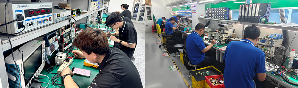
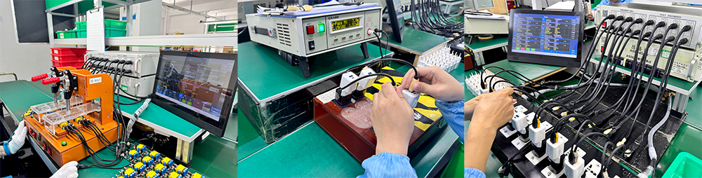
Step 13 — Functional Testing: Every Charger Must Prove It Works
Before leaving the production line, every charger should undergo functional verification.
Unlike engineering validation, which evaluates the design, production testing confirms that each manufactured unit operates correctly.
Typical functional tests include:
• AC input verification
• Output voltage accuracy
• USB-C Power Delivery negotiation
• PPS voltage switching
• Multi-port power allocation
• Protection circuit activation
• No-load power consumption
• Full-load output verification
Testing every production unit helps identify assembly defects before products reach customers.
Step 14 — Aging Tests: Screening Out Early Failures
Even if a charger passes functional testing, professional manufacturers often perform an additional aging or burn-in process.
During aging tests, chargers operate continuously under controlled load and temperature conditions for several hours.
This process helps identify components that may fail early in their service life.
Common objectives include:
• Detecting unstable components
• Verifying thermal stability
• Confirming output consistency
• Screening for early-life failures
• Validating long-duration operation
Aging tests do not guarantee that a charger will never fail, but they significantly improve confidence in production quality.

Step 15 — Final Quality Inspection Before Shipment
Before packaging, finished chargers undergo a final quality inspection.
Inspectors verify:
• Cosmetic appearance
• Label accuracy
• Certification markings
• Mechanical integrity
• Functional performance
• Packaging completeness
Random sampling may also include additional reliability checks to ensure ongoing production consistency.
For OEM customers, this final stage provides confidence that products shipped under their brand meet the agreed quality standard.
From the Factory Floor
One detail often overlooked by customers is that engineering doesn't stop once production begins.
During mass production, manufacturing engineers continuously collect data from testing stations, monitor defect trends and review customer feedback.
If recurring issues are detected—even minor ones—the engineering team may revise work instructions, optimize assembly methods or adjust component specifications.
This continuous improvement cycle allows a charger platform to become more reliable over time without changing its core design.

Why Manufacturing Consistency Is a Competitive Advantage
For OEM and ODM projects, buyers are rarely concerned about just one successful prototype.
They need confidence that the 10th charger, the 10,000th charger and the 100,000th charger will perform with the same reliability.
Achieving this level of consistency requires more than modern equipment.
It requires standardized processes, disciplined quality management and close collaboration between engineering and manufacturing teams.
This is one of the defining characteristics of experienced charger manufacturers.
From Engineering Excellence to Long-Term Reliability
Every USB-C charger begins as an idea.
It evolves through circuit simulations, component selection, transformer calculations, PCB layout optimization and firmware development before becoming a working prototype.
But professional charger engineering doesn't stop when the first prototype powers on.
It continues through thermal analysis, EMI optimization, engineering validation, manufacturing reviews, reliability testing and production quality control.
Each stage builds upon the previous one.
Skip one step, and problems often appear later—sometimes during certification, sometimes in production, and sometimes only after customers have been using the product for months.
This is why experienced charger manufacturers invest heavily in engineering long before products reach the assembly line.
Their goal isn't simply to build a charger that works.
It's to build one that continues to perform safely and consistently throughout its entire service life.
From the Factory Floor
One lesson we've learned through years of charger development is that no engineering drawing remains perfect forever.
During pilot production, small improvements are almost always discovered.
Sometimes an engineer notices that moving a capacitor a few millimeters improves thermal airflow.
Sometimes a production technician suggests a more reliable assembly sequence.
Occasionally, long-term reliability testing reveals that changing a transformer winding method reduces operating temperatures by several degrees.
None of these changes dramatically alter the appearance of the charger.
Yet together they contribute to a product that is easier to manufacture, more reliable in daily use and more consistent across large production volumes.
This continuous improvement mindset is one of the defining characteristics of mature charger engineering.
Final Thoughts
Designing a modern USB-C charger is a multidisciplinary engineering process.
It combines power electronics, embedded control, thermal engineering, mechanical design, manufacturing engineering and quality management into a single product that most people use every day without thinking twice.
Behind every compact GaN charger lies countless engineering decisions.
Every PCB trace.
Every transformer winding.
Every protection circuit.
Every firmware adjustment.
Every production checkpoint.
These details are rarely visible to the user, but they determine whether a charger remains safe, efficient and reliable over years of daily operation.
For OEM brands, distributors and procurement teams, understanding this process is equally important.
Choosing a charger manufacturer should never be based solely on price or specifications.
The true value lies in the engineering capability behind the product—and in the factory's ability to reproduce that quality consistently at scale.
Frequently Asked Questions (FAQ)
Q1: What is the first step in designing a USB-C charger?
A: Professional charger design begins with defining product requirements, including power output, supported charging protocols, target devices, certification requirements and physical size constraints.
Q2: Why is transformer design so important in a charger?
A: The transformer provides electrical isolation and transfers energy from the primary to the secondary circuit. Its design directly affects efficiency, thermal performance, safety and overall charger size.
Q3: What is the role of PCB layout in charger performance?
A: PCB layout influences current flow, heat distribution, electromagnetic interference (EMI), electrical safety and long-term reliability. Even with the same components, a poor layout can reduce overall performance.
Q4: What is the difference between EVT, DVT and PVT?
A: EVT (Engineering Validation Test): Verifies that the circuit design works correctly.
DVT (Design Validation Test): Confirms that the finished product meets electrical, mechanical and environmental requirements.
PVT (Production Validation Test): Ensures the product can be manufactured consistently at scale.
Q5: Why do modern USB-C chargers require firmware?
A: Unlike older fixed-voltage chargers, USB-C Power Delivery chargers must communicate with connected devices to negotiate voltage, current and power levels. Firmware manages this communication and enables advanced charging features such as PPS and PD3.1.
Q6: Why are thermal simulations performed before production?
A: Thermal simulations help engineers predict heat distribution, identify potential hotspots and optimize cooling before physical prototypes are built, reducing development time and improving product reliability.
Q7: How do professional charger factories maintain consistent quality?
A: Professional factories combine incoming material inspection, automated SMT production, AOI inspection, functional testing, aging tests and final quality audits to ensure every production batch matches the validated engineering design.