How EMI Affects Charger Performance: Engineering Stable, Safe and Compliant USB-C Chargers
Quick Answer (Featured Snippet)
Electromagnetic interference (EMI) is unwanted electrical noise generated by high-frequency switching circuits inside a charger. If not properly controlled, EMI can reduce charging stability, interfere with nearby electronic devices, increase certification failures and negatively affect long-term reliability. Professional charger manufacturers reduce EMI through optimized PCB layout, transformer design, grounding strategy, filtering circuits and extensive EMC testing before mass production.
Key Takeaways
• Every switching charger generates electromagnetic interference.
• EMI cannot be eliminated, but it can be effectively controlled through engineering.
• PCB layout, transformer construction and filter design work together to reduce EMI.
• Poor EMI control often results in certification failures and repeated prototype revisions.
• Professional charger factories consider EMI from the earliest stages of product • development rather than treating it as a final testing issue.
Introduction
Modern USB-C chargers are remarkably compact.
A charger that fits comfortably in your pocket can now deliver 65W, 100W or even 140W of power while supporting multiple charging protocols.
This level of performance is only possible because today's chargers operate at very high switching frequencies.
However, every improvement comes with a trade-off.
Higher switching frequencies improve efficiency and reduce transformer size, but they also generate unwanted electrical noise.
Engineers refer to this noise as electromagnetic interference, or EMI.
Although users rarely notice EMI directly, it is one of the biggest engineering challenges behind every modern charger.
Poor EMI control can affect much more than certification results.
It may increase signal instability, reduce charging consistency, interfere with nearby electronics and even contribute to additional heat generation inside the charger.
For engineers, reducing EMI is not about solving a single problem.
It is about balancing efficiency, safety, thermal performance, manufacturability and regulatory compliance—all at the same time.
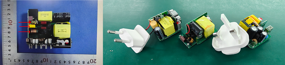
What Is EMI?
EMI refers to unwanted electromagnetic energy generated during normal circuit operation.
Inside a fast charger, power devices switch on and off hundreds of thousands of times every second.
Every switching event creates rapidly changing voltages and currents.
These rapid transitions generate electromagnetic energy that spreads through:
• PCB traces
• Transformer windings
• Power cables
• Internal wiring
• The surrounding air
Not all of this energy reaches your devices.
Much of it remains inside the charger.
However, if the design is not properly optimized, some of this noise can escape and interfere with nearby electronic equipment.
That is why every charger sold in regulated markets must comply with strict EMC (Electromagnetic Compatibility) standards before it can be certified.

Read More
EMI Is a Natural Byproduct of High-Speed Power Conversion
Many people mistakenly believe that EMI is caused by poor manufacturing.
In reality, every switching power supply generates EMI.
Even the highest-quality charger from a leading global brand produces electromagnetic noise.
The difference lies in how effectively that noise is managed.
Professional engineers focus on reducing EMI to acceptable levels rather than attempting to eliminate it entirely.
As charging power increases, EMI control becomes even more challenging.
A compact 20W charger may be relatively straightforward to optimize.
A 100W multi-port GaN charger, however, contains:
• Higher switching currents
• More complex PCB routing
• Additional communication circuits
• Greater thermal density
• Multiple power conversion paths
Each of these factors increases the complexity of EMI optimization.
Conducted EMI vs Radiated EMI
Engineers generally classify EMI into two categories.
Conducted EMI
Conducted EMI travels through electrical conductors such as power lines and USB cables.
This type of interference can return to the AC mains or reach connected electronic devices.
International EMC testing places significant emphasis on conducted emissions because excessive noise may affect other products connected to the same electrical network.
Radiated EMI
Radiated EMI spreads through electromagnetic fields.
In simple terms, parts of the charger begin acting like tiny antennas.
Poor PCB routing, oversized switching loops or inadequate grounding can all increase radiated emissions.
Although users cannot see these electromagnetic fields, testing equipment can measure them with remarkable precision.
Both types of EMI must be controlled before a charger can successfully pass certification.
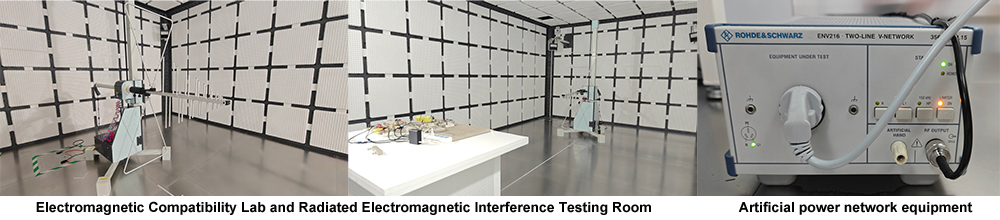
Where Does EMI Come From Inside a Charger?
EMI is not generated by a single component.
Instead, it results from the interaction of multiple parts working together.
Several major sources contribute to EMI.
High-Speed Switching Devices
Modern GaN transistors and MOSFETs switch extremely quickly.
Fast switching improves efficiency but also increases voltage transition speed (dv/dt) and current transition speed (di/dt), both of which contribute to electromagnetic noise.
Ironically, the technology that enables smaller chargers also requires more sophisticated EMI engineering.
Transformer
As discussed in the previous article, the transformer transfers energy through changing magnetic fields.
These magnetic fields are essential for operation, but they also become a potential source of electromagnetic emissions if winding structure, shielding or magnetic coupling are not properly optimized.
Transformer design and EMI performance are therefore closely linked.
PCB Layout
One of the largest contributors to EMI is PCB layout.
Long switching loops, poor return current paths and fragmented ground planes increase unwanted electromagnetic radiation.
This explains why PCB layout reviews are performed long before EMC testing begins.
Correcting layout problems during design is far easier than redesigning hardware after certification testing.
USB-C Output Circuit
Although output voltages are much lower than primary-side switching voltages, USB-C communication circuits still require careful routing.
Stable Power Delivery communication depends on maintaining clean signal integrity while avoiding interference from nearby switching circuits.
Why EMI Affects More Than Certification
Many procurement teams assume EMI matters only because certification laboratories require EMC testing.
In practice, EMI influences product quality in several other ways.
Poor EMI control may lead to:
• Reduced charging stability
• Intermittent USB PD negotiation failures
• Increased operating temperature
• Higher switching losses
• Audible electrical noise
• Reduced long-term reliability
These issues may not appear immediately.
Instead, they often emerge during extended operation or under demanding charging conditions.
This is one reason why professional manufacturers perform repeated validation testing rather than relying on a single certification report.
EMI Control Begins During Product Design
A common misconception is that EMI is solved by adding more filter components after a prototype fails testing.
Experienced engineers rarely work this way.
Successful EMI control starts at the beginning of product development.
When defining the PCB architecture, engineers already consider:
• Switching current paths
• Ground return strategy
• Transformer placement
• Filter positioning
• Safety spacing
• High-frequency loop size
By integrating these principles into the initial design, the likelihood of passing EMC testing increases significantly.
Attempting to solve EMI only after hardware has been completed often requires expensive redesigns and additional prototype cycles.
PCB Layout Plays a Bigger Role Than Many Expect
In the previous article, we discussed how PCB layout influences efficiency and thermal performance.
Its impact on EMI is equally significant.
Engineers carefully reduce the area enclosed by high-frequency switching loops because larger loops radiate more electromagnetic energy.
Ground planes are designed to provide controlled return paths, helping reduce noise while improving signal stability.
Sensitive control circuits are physically separated from noisy power stages to prevent interference.
These decisions may appear minor individually, but together they form the foundation of effective EMC performance.
For experienced hardware engineers, successful EMI optimization begins long before the first prototype is assembled.
How EMI Filters Work Inside USB-C Chargers
Once engineers understand where electromagnetic interference originates, the next challenge is preventing that noise from leaving the charger.
Contrary to what many people imagine, an EMI filter is not a single component. It is a carefully designed network made up of inductors, capacitors and protective components that work together to suppress unwanted high-frequency noise while allowing normal AC power to pass through.
Think of it as a traffic management system.
Electricity at 50Hz or 60Hz—the frequency supplied by household power—is allowed to flow freely into the charger. High-frequency switching noise, however, is slowed down, redirected or absorbed before it can travel back into the power grid or interfere with nearby electronics.
A typical USB-C charger EMI filter may include:
• Common-mode choke
• Differential-mode inductor
• X capacitor
• Y capacitors
• MOV surge protection
• Fuse
Each component performs a different function, and removing even one can significantly reduce EMC performance.
This is why professionally engineered chargers often contain a more sophisticated input stage than low-cost, non-certified products.
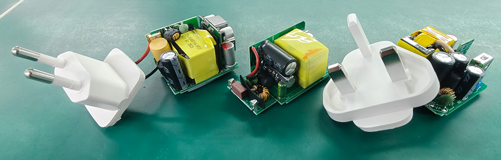
Why PCB Layout and EMI Filters Must Work Together
One of the biggest misconceptions in charger design is believing that adding larger EMI filters will automatically solve EMC problems.
In reality, filters should be viewed as the final layer of defense—not the primary solution.
Imagine a PCB with oversized switching loops and poor grounding. Even the highest-quality EMI filter will struggle to compensate for excessive noise generated inside the circuit.
Professional engineers therefore follow a clear design philosophy:
Reduce noise at its source before attempting to filter it.
This involves:
• Keeping high-frequency current loops as small as possible.
• Optimizing transformer coupling.
• Designing continuous ground reference planes.
• Separating noisy power stages from sensitive control circuits.
• Carefully positioning EMI filter components close to the AC input.
Only after these fundamentals are optimized does the EMI filter achieve its full effectiveness.
For this reason, experienced hardware teams review PCB layout and EMI filter design simultaneously rather than treating them as independent tasks.
Common EMI Design Mistakes in Charger Development
Every charger development project presents unique challenges, but several EMI-related problems appear repeatedly during engineering reviews.
1. Switching Loops That Are Too Large
Large switching loops radiate more electromagnetic energy.
Reducing loop area is one of the simplest and most effective ways to improve EMC performance.
2. Improper Grounding Strategy
Poor ground connections can increase common-mode noise, destabilize control circuits and create unpredictable EMC test results.
Ground design is therefore planned from the earliest PCB layout stage rather than adjusted after prototype testing.
3. Transformer Placement
Even an excellent transformer can contribute to EMI if it is positioned too close to sensitive circuits or routed improperly on the PCB.
Mechanical placement and electrical design must work together.
4. Incomplete EMI Filter Design
Some low-cost chargers reduce manufacturing costs by simplifying or omitting parts of the EMI filter network.
While the charger may still function, it is far more likely to experience EMC failures or unstable operation under demanding conditions.
5. Focusing Only on Certification
Passing an EMC test once does not necessarily guarantee consistent product quality.
A robust charger should maintain stable EMI performance across different production batches, operating temperatures and input voltages.
This consistency depends on engineering discipline, manufacturing control and component quality—not certification alone.
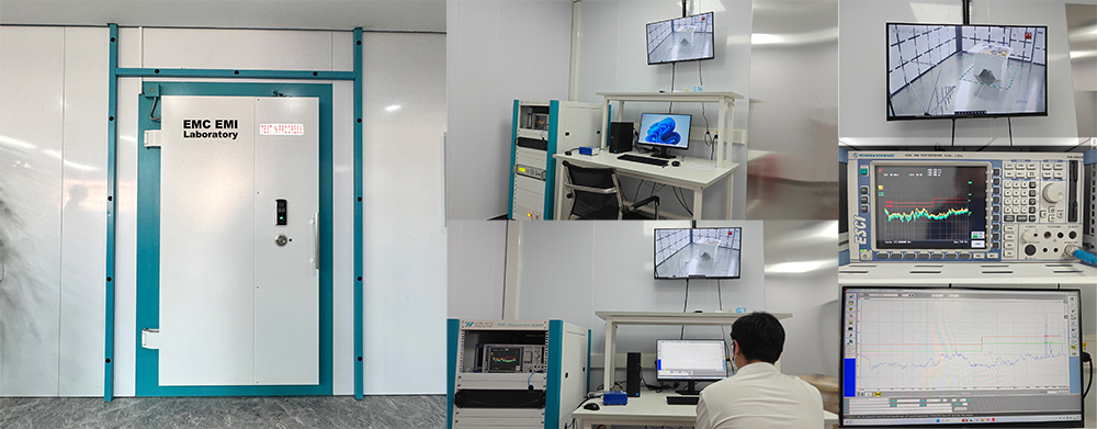
How Professional Charger Manufacturers Validate EMI Performance
EMI optimization does not end when the PCB is completed.
Professional charger manufacturers verify EMC performance throughout product development.
A typical validation process includes:
Engineering Simulation
Before the first prototype is built, engineers review switching loops, grounding paths, transformer placement and filter locations using circuit design and PCB layout tools.
Prototype Evaluation
Early hardware samples are tested under different operating conditions to identify unexpected noise sources.
Engineers often use oscilloscopes, spectrum analyzers and current probes to observe switching behavior in real time.
Pre-Compliance Testing
Rather than waiting for formal certification, many manufacturers perform internal EMC evaluations that closely replicate laboratory conditions.
This allows potential problems to be corrected before official testing.
Certification Testing
Products intended for global markets typically undergo EMC testing according to regional regulations before entering mass production.
Depending on the destination market, this may involve CE, FCC, UKCA, KC or other applicable certification requirements.
Production Verification
Even after certification has been achieved, manufacturers continue monitoring production quality.
Periodic verification ensures that component variation, supplier changes or manufacturing tolerances do not negatively affect EMC performance.
-universal-charging-for-laptop-samsung-iphone-fast-charger-zx-3u43t.jpg)
Read More
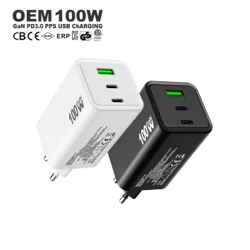
Designed for OEM charger manufacturing and brand customization, this 100W USB-C wall charger combines high output power, intelligent power distribution, and compact GaN design, making it ideal for modern users who require efficient charging across smartphones, tablets, and laptops.
Read More
Why EMI Engineering Reflects a Manufacturer's Technical Capability
Many aspects of charger quality can be seen from the outside.
Power rating, USB ports and product dimensions are immediately visible.
EMI engineering is different.
Most of the work happens long before the charger reaches the customer.
A manufacturer that consistently produces chargers with stable EMC performance usually demonstrates strengths in several areas:
• Hardware engineering
• PCB layout optimization
• Magnetic component design
• Prototype validation
• Quality management
• Manufacturing consistency
These capabilities are difficult to measure from a specification sheet alone, yet they play a significant role in long-term product reliability.
For OEM and ODM customers, understanding how a supplier approaches EMI engineering provides valuable insight into the overall maturity of its product development process.
Final Thoughts
Electromagnetic interference is an unavoidable part of every modern switching charger.
The objective is not to eliminate EMI completely, but to control it through intelligent engineering.
Achieving this requires much more than adding filter components.
Successful EMI optimization combines thoughtful PCB layout, carefully designed transformers, effective grounding strategies, properly selected filter circuits and rigorous validation throughout the entire development process.
As USB-C charging continues moving toward higher power levels and more compact GaN designs, EMI engineering will become increasingly important.
For professional charger manufacturers, excellent EMC performance is not the result of luck or last-minute adjustments—it is the outcome of systematic engineering decisions made from the very beginning of product development.
Frequently Asked Questions (FAQ)
Q1: What is EMI in a USB-C charger?
EMI (Electromagnetic Interference) is high-frequency electrical noise generated by switching circuits during normal charger operation.
Q2: Can EMI damage electronic devices?
Certified chargers are designed to keep EMI within regulated limits. Poorly designed or uncertified products may create interference that affects nearby electronic equipment.
Q3: What is the difference between EMI and EMC?
EMI refers to the unwanted electrical noise itself, while EMC (Electromagnetic Compatibility) describes a product's ability to operate correctly without causing or suffering from excessive interference.
Q4: Why do GaN chargers require better EMI control?
GaN devices switch faster than conventional silicon components, creating steeper voltage transitions that require more sophisticated EMI management.
Q5: What components are commonly used in an EMI filter?
Common-mode chokes, X capacitors, Y capacitors, differential inductors, MOVs and fuses are commonly used.
Q6: Does PCB layout influence EMI?
Yes. PCB layout is one of the most important factors affecting EMI performance because it determines current paths, grounding quality and loop area.
Q7: How do charger manufacturers test EMI?
Manufacturers perform engineering simulations, prototype validation, pre-compliance testing and formal EMC certification before mass production.
Q8: Why is EMI important for OEM charger buyers?
Good EMI engineering improves certification success, charging stability, product reliability and manufacturing consistency across production batches.
Gan Charger Engineering Article
• How PCB Layout Determines Charger Performance: Inside the Engineering Behind Fast Chargers.↗
• How Transformer Design Determines Charger Efficiency: The Engineering Behind Every Fast Charger.↗
• How a USB-C Charger Is Designed: From Circuit Concept to Mass Production.↗
• CISPR 32 Standard for Multimedia Equipment EMC.↗
Read More