How Flyback Converters Work in USB-C Chargers: The Power Conversion Technology Behind Fast Charging
Quick Answer (Featured Snippet)
A flyback converter is the most widely used power conversion topology in USB-C chargers. It converts high-voltage AC power into stable low-voltage DC output while providing electrical isolation between the mains supply and connected devices. Modern flyback designs combine high efficiency, compact size and excellent cost-performance, making them ideal for USB PD and GaN fast chargers from 20W to over 100W.
Key Takeaways
• Most USB-C wall chargers use a flyback converter.
• The flyback circuit controls how electrical energy is stored and released during each switching cycle.
• Modern GaN chargers still rely on flyback topology, although the switching devices have changed.
• Transformer design, PCB layout and controller IC selection all influence flyback performance.
• A well-optimized flyback converter improves efficiency, reduces heat and enhances long-term reliability.
Introduction
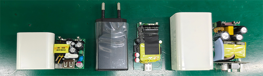
When people open a fast charger for the first time, they often recognize familiar components such as the transformer, capacitors or USB-C controller.
What they don't see is something equally important—the way these components work together.
That "way of working together" is known as the power topology.
Think of it as the overall architecture of the power supply.
The same transformer can perform very differently depending on how energy is controlled.
The same GaN transistor can deliver completely different efficiency depending on the switching circuit that drives it.
In other words, components are important, but topology determines how those components behave as a complete system.
Among all power supply topologies used today, one design remains the clear industry standard for compact USB-C chargers:
The flyback converter.
Whether you're charging a smartphone, tablet or laptop, there is a very good chance the charger in your hand is built around a flyback architecture.
Its popularity isn't accidental.
Over decades of development, engineers have refined flyback converters into a solution that balances efficiency, safety, size and manufacturing cost remarkably well.
Understanding how this topology works helps explain why modern chargers can deliver more power from increasingly smaller enclosures.
What Is a Flyback Converter?
Despite its technical name, the operating principle of a flyback converter is surprisingly intuitive.
Instead of transferring energy continuously from the input to the output, a flyback converter works in two distinct stages.
First, energy is stored inside the transformer's magnetic field.
Then, that stored energy is released to the output.
This rapid cycle repeats hundreds of thousands of times every second.
Because each switching cycle stores and releases only a small amount of energy, the output appears smooth and continuous to the connected device.
This approach allows engineers to combine voltage conversion and electrical isolation into a single compact magnetic component.
That simplicity is one reason flyback converters dominate consumer charger design.
Following One Complete Switching Cycle
Rather than thinking about electricity flowing continuously, it helps to imagine the flyback converter working in repeated pulses.
Stage One: Energy Storage
When the primary switching device turns on, current begins flowing through the transformer's primary winding.
Instead of immediately reaching the USB output, this energy is temporarily stored inside the magnetic core.
During this stage, the secondary side remains inactive.
The transformer is effectively "charging itself."
Stage Two: Energy Release
When the switching device turns off, the magnetic field inside the transformer collapses.
The stored energy now flows through the secondary winding toward the output circuit.
Capacitors smooth the pulses into stable DC power suitable for USB Power Delivery.
This process repeats continuously at extremely high speed.
Although each switching cycle lasts only microseconds, together they create the stable charging experience users expect.
Why Flyback Topology Became the Industry Standard
Not every power supply uses a flyback converter.
Other architectures such as forward converters, half-bridge converters and LLC resonant converters each have their own advantages.
So why has flyback remained the preferred choice for most USB-C chargers?
The answer lies in balance.
For compact consumer chargers, engineers must satisfy several requirements simultaneously:
• High efficiency
• Small size
• Electrical isolation
• Reasonable manufacturing cost
• Stable USB PD performance
• Reliable mass production
Flyback topology achieves all of these surprisingly well.
Unlike more complex architectures, it requires fewer magnetic components and a relatively simple control circuit.
This reduces manufacturing complexity while maintaining excellent performance across a wide range of output powers.
For this reason, flyback designs continue to dominate chargers from 20W smartphone adapters to many 100W laptop chargers.
How the Flyback Converter Works with Modern GaN Technology
Some people assume that GaN technology has replaced flyback converters.
In reality, these two technologies serve different purposes.
A flyback converter describes the power conversion architecture.
GaN refers to the switching device used within that architecture.
Replacing a traditional silicon MOSFET with a GaN transistor does not fundamentally change how the flyback converter operates.
Instead, it allows the converter to switch faster and more efficiently.
Higher switching frequencies enable engineers to:
• Reduce transformer size.
• Improve power density.
• Lower switching losses.
• Increase overall efficiency.
• Build more compact chargers.
However, these benefits also require more sophisticated engineering.
Faster switching introduces greater EMI challenges, tighter PCB layout requirements and more demanding thermal design.
In other words, GaN improves the flyback converter—but it also raises the engineering standard needed to implement it successfully.
Every Flyback Converter Depends on System-Level Design
One reason professional charger development is so complex is that no component operates independently.
The flyback converter relies on close coordination between multiple engineering disciplines.
For example:
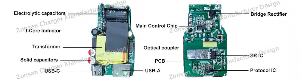
• The transformer stores and transfers energy.
• The PCB layout minimizes switching losses and EMI.
• The controller IC regulates switching behavior.
• The feedback circuit maintains stable output voltage.
• The EMI filter suppresses high-frequency noise.
• The thermal design keeps temperatures within safe operating limits.
If any one of these subsystems is poorly designed, the overall converter suffers.
This is why experienced engineering teams evaluate the flyback converter as an integrated system rather than optimizing each component in isolation.
Not Every Flyback Converter Performs the Same
Although many chargers use flyback topology, performance varies significantly.
Two chargers may both advertise 65W USB PD output and use similar components, yet one operates cooler, charges more efficiently and passes EMC testing with fewer design revisions.
Why?
Because the topology itself is only the starting point.
Real-world performance depends on dozens of engineering decisions, including:
• Transformer optimization
• Switching frequency selection
• Snubber circuit design
• PCB routing
• Component placement
• Feedback compensation
• Thermal management
• Manufacturing consistency
This explains why experienced OEM buyers increasingly evaluate engineering capability rather than simply comparing component lists.
A mature flyback design reflects the quality of the entire development process—not just the specification sheet.
Quasi-Resonant (QR) Flyback vs Traditional Flyback
As USB-C charging power continued to increase, engineers began looking for ways to improve the efficiency of conventional flyback converters without significantly increasing circuit complexity.
One of the most successful solutions is the Quasi-Resonant (QR) Flyback Converter.
Rather than switching at a fixed frequency throughout the entire operating cycle, a QR flyback controller monitors the transformer's behavior and turns the switching device on at the most favorable moment—typically when the drain voltage reaches a valley.
This technique, commonly called Valley Switching, reduces switching losses because the transistor changes state when voltage stress is lower.
The advantages are significant:
• Higher conversion efficiency
• Lower switching losses
• Reduced operating temperature
• Lower EMI emissions
• Improved performance under varying loads
For these reasons, QR flyback has become the preferred architecture for many premium USB-C chargers between 30W and 100W.
However, QR control also introduces additional engineering considerations.
Because switching frequency changes dynamically with operating conditions, engineers must carefully optimize transformer design, compensation networks and PCB layout to maintain stable performance across the entire load range.
The result is a charger that is more efficient—but also more demanding to develop.
What Is Active Clamp Flyback (ACF)?
As fast charging continues moving toward 100W, 140W and even higher power levels, another flyback architecture has become increasingly important:
Active Clamp Flyback (ACF).
Compared with traditional flyback designs, ACF introduces an additional active switch and clamp circuit.
Instead of allowing leakage energy from the transformer to dissipate as heat, the active clamp recovers part of that energy and redirects it back into the conversion process.
This seemingly small improvement produces several important benefits:
• Higher overall efficiency
• Reduced switching stress
• Lower voltage spikes
• Improved thermal performance
• Higher achievable switching frequency
• Better suitability for compact high-power GaN chargers
Many modern 100W to 140W GaN chargers now employ Active Clamp Flyback because it helps achieve demanding efficiency targets while maintaining compact product dimensions.
That said, ACF is not simply a "better flyback."
It is a more sophisticated architecture requiring:
• More complex control algorithms
• Additional power devices
• More demanding PCB layout
• Tighter timing optimization
• Greater engineering expertise
For entry-level chargers, the additional cost and complexity may outweigh the performance benefits.
Choosing between traditional flyback, QR flyback and ACF therefore depends on the product's design goals rather than following a single universal solution.
-universal-charging-for-laptop-samsung-iphone-fast-charger-zx-3u43t.jpg)
Read More
Common Challenges When Designing a Flyback Charger
Although the flyback converter appears relatively simple compared with other power topologies, designing a high-performance charger around it is far from straightforward.
In practice, engineers must solve several interconnected challenges simultaneously.
Maintaining High Efficiency Across Different Loads
Users rarely operate chargers under a single fixed condition.
A charger may spend part of the day charging wireless earbuds at only a few watts, then switch to powering a laptop at full output.
Maintaining high efficiency across such a wide operating range requires careful controller selection, optimized transformer parameters and well-tuned feedback compensation.
Managing Heat Inside a Compact Enclosure
As charger dimensions become smaller, internal component spacing decreases.
Heat generated by the switching devices, transformer and output rectifiers can quickly accumulate.
Effective thermal management therefore depends not only on component selection but also on enclosure design, copper distribution, airflow paths and thermal interface materials.
Achieving Stable USB Power Delivery Communication
Modern USB-C chargers do much more than provide voltage.
They continuously communicate with connected devices through the USB Power Delivery protocol.
Power conversion circuits must therefore remain electrically stable while supporting rapid voltage transitions, dynamic power negotiation and multiple charging profiles.
Even small disturbances in the power stage can affect protocol stability if the design is not carefully optimized.
Passing International EMC Certification
As discussed in the previous article, higher switching frequencies increase EMI challenges.
The flyback converter, transformer, PCB layout and filter circuits must all work together to satisfy EMC requirements for different global markets.
Engineering teams often perform several rounds of pre-compliance testing before submitting products for official certification.
Why Controller IC Selection Is Just as Important as the Topology
When discussing charger design, attention often focuses on visible components such as transformers or GaN transistors.
However, one of the most influential devices inside the entire charger is the controller IC.
The controller determines:
• Switching frequency
• Startup sequence
• Protection functions
• Soft-start behavior
• Output regulation
• Burst mode operation
• Fault response
In other words, the controller acts as the "brain" of the flyback converter.
Even an excellent transformer and carefully optimized PCB cannot deliver their full potential if the controller is poorly matched to the application.
For this reason, experienced charger manufacturers evaluate controller ICs not only by their datasheets but also through extensive prototype testing under real operating conditions.

How Professional Charger Manufacturers Optimize Flyback Circuits
Developing a commercially successful charger involves far more than selecting a flyback controller reference design.
Professional manufacturers follow a structured engineering process that gradually refines every aspect of the power stage.
This typically includes:
Simulation and Architecture Evaluation
Engineers begin by selecting the most appropriate topology based on target power, efficiency goals, enclosure size and cost objectives.
Magnetic Optimization
Transformer parameters are adjusted to achieve the desired balance between efficiency, thermal performance and EMI.
PCB Layout Optimization
Switching loops, current return paths and grounding structures are refined to reduce electrical losses and improve EMC performance.
Prototype Validation
Multiple engineering samples are evaluated under different input voltages, temperatures and loading conditions.
Design adjustments continue until performance targets are consistently achieved.
Reliability Verification
Before production begins, chargers undergo extensive reliability testing, including:
• Continuous aging tests
• Full-load operation
• Thermal cycling
• High-humidity testing
• Component stress evaluation
Only after these validation stages are complete does the project move into mass production.
This disciplined engineering process is one of the defining characteristics of an experienced USB-C charger manufacturer.
Read More
Final Thoughts
The flyback converter has remained the foundation of modern charger design for a reason.
Its ability to combine electrical isolation, compact size, excellent efficiency and cost-effective manufacturing has made it the preferred topology for millions of USB-C chargers worldwide.
Yet the topology itself is only the beginning.
The real performance of a charger depends on how successfully engineers integrate transformer design, controller selection, PCB layout, EMI optimization, thermal management and manufacturing quality into one cohesive system.
As charging technologies continue to evolve, flyback architectures such as QR Flyback and Active Clamp Flyback will play an increasingly important role in delivering higher power levels without sacrificing efficiency or reliability.
For OEM and ODM customers, understanding these engineering principles provides valuable insight into the technical capabilities behind every professional charger manufacturer.

Read More
Frequently Asked Questions (FAQ)
Q1: What is a flyback converter?
A flyback converter is an isolated switching power supply topology that stores energy in a transformer and releases it to the output during each switching cycle.
Q2: Why is flyback topology commonly used in USB-C chargers?
It offers an excellent balance of efficiency, compact size, electrical isolation and manufacturing cost, making it ideal for fast chargers.
Q3: Is GaN a replacement for flyback topology?
No. GaN is a semiconductor technology, while flyback is a power conversion architecture. Many GaN chargers still use flyback converters.
Q4: What is QR Flyback?
Quasi-Resonant Flyback uses valley switching to reduce switching losses, improve efficiency and lower EMI compared with conventional fixed-frequency flyback converters.
Q5: What is Active Clamp Flyback?
Active Clamp Flyback (ACF) recovers transformer leakage energy, improving efficiency and reducing switching stress in high-power chargers.
Q6: Does flyback topology affect charger efficiency?
Yes. Together with transformer design, controller IC selection and PCB layout, flyback architecture has a significant influence on efficiency and thermal performance.
Q7: Can flyback converters support 100W USB-C charging?
Yes. Modern QR Flyback and Active Clamp Flyback designs are widely used in 100W USB PD and GaN chargers.
Q8: How do manufacturers validate flyback charger performance?
Through engineering simulations, prototype testing, EMC verification, thermal analysis, reliability testing and production validation.
Recommended
• How Transformer Design Determines Charger Efficiency: The Engineering Behind Every Fast Charger.↗
• How EMI Affects Charger Performance: Engineering Stable, Safe and Compliant USB-C Chargers.↗
• How PCB Layout Determines Charger Performance: Inside the Engineering Behind Fast Chargers.↗