From PCB Design to Mass Production: How Custom Chargers Are Engineered
A custom charger does not go directly from an idea to a production line.
The usual engineering path is: Product Requirements → Circuit Design → PCB Layout → Prototype → Engineering Validation → Tooling → DVT → PVT → Mass Production.
At each stage, engineers verify something different.
The PCB must work electrically. The power system must remain stable under load. The housing must manage heat. The USB-C PD protocol must communicate correctly with devices. The final design must also be suitable for certification and repeatable mass production.
This is why choosing an experienced charger manufacturer matters for OEM and ODM projects. A factory that only assembles products may be able to manufacture an existing charger, but developing a new 65W, 100W or 140W charger requires much deeper engineering capability.

A customer may come to a factory with a simple requirement: “We need a compact 65W USB-C GaN charger with two USB-C ports.”
From a buyer's point of view, this sounds like a product specification.
From an charger engineer's point of view, it is only the beginning.
The team still needs to answer questions such as:
• What power architecture should be used?
• Which GaN components are suitable?
• What PD profiles are required?
• Does the charger need PPS?
• How much power should each USB-C port provide?
• What is the target size?
• How will heat leave the housing?
• What certification standards apply?
• Can the PCB fit inside the proposed housing?
• Can the design be manufactured consistently?
• Can the product pass reliability testing?
The answers affect one another.
A smaller housing can make thermal management harder. A higher power target can require a different power architecture.
Adding another USB-C port can change the PCB layout and power allocation. Changing the housing can affect component placement.
That is why charger development is an engineering process rather than simply a production process.
The Complete Journey From PCB Design to Mass Production
For a custom charger project, the development process can be simplified into several major stages:
Stage 1 — Product Requirements: Define what the charger needs to do.
Stage 2 — Electrical Architecture: Select the power topology, controller and key components.
Stage 3 — PCB Design: Turn the electrical concept into a physical circuit board.
Stage 4 — Prototype: Build the first engineering samples.
Stage 5 — Engineering Validation: Test electrical, thermal, protocol and mechanical performance.
Stage 6 — Design Optimization: Fix problems discovered during testing.
Stage 7 — Tooling and DVT: Validate the production-intent design.
Stage 8 — PVT: Confirm that the manufacturing process can repeatedly produce acceptable units.
Stage 9 — Mass Production: Release the approved design into regular production.
The exact terminology can vary between companies, but the principle is similar.
You do not want to discover a fundamental design problem after the production line has already been set up.
* How long does it take to develop a custom charger?
Step 1: Start With the Product Requirements
Before an engineer draws the first PCB trace, the product requirements need to be clear.
A good specification might look like this:
Product: 65W GaN USB-C Charger
Ports: 2 × USB-C
Power: 65W total
Protocols: PD + PPS
Input: 100–240V AC
Plug: EU
Target Markets: Europe, UK and South Korea
Housing: Custom
Branding: Private label
Certification: CE / RoHS / CB / FCC / ERP / KC / UKCA
This is much more useful than simply saying: “Please make a 65W fast charger.” The more clearly the product requirements are defined, the fewer major changes are likely to happen later.
Power Rating Is Only One Part of the Specification
A charger may be called: 20W charger, 25W charger, 30W charger, 45W charger, 65W charger, 100W charger, 140W charger and 240w up.
But the wattage does not define the complete product.
For example, two 65W chargers can have very different designs.
One might be: 1 × USB-C / 65W
Another could be: 2 × USB-C or 1C1A / 65W total
Another could be: 2C1A / 65W total
The power allocation, PCB design, thermal behavior and protocol requirements will all be different.
This is particularly important for buyers looking for a 65W charger manufacturer. A supplier's experience with a single-port 65W charger does not necessarily mean it has the same experience with a compact multi-port 65W platform.
Step 2: Define the Electrical Architecture
Once the product requirements are confirmed, engineers determine the basic electrical architecture.
A modern charger can include several functional sections:
AC Input → Protection → Rectification → Power Conversion → Transformer / Isolation → Secondary Rectification → Output Filtering → USB-C PD / PPS Control → Device
The actual topology depends on the power level and product design. For a compact GaN charger, the engineering team may use a high-frequency switching architecture to achieve greater power density.
The important point is that the architecture needs to be selected before detailed PCB design begins.
Why Component Selection Happens Before PCB Layout
A PCB is not designed around empty spaces. Charger Engineers need to know the approximate size, electrical characteristics and thermal behavior of the major components first.
Depending on the charger, this can include:
• Power ICs
• GaN power devices
• Transformers
• Capacitors
• Inductors
• Rectifiers
• USB-C controllers
• Protection components
• Connectors
• Thermal components
Component selection also involves supply considerations. A component may perform well technically but be difficult to source consistently.
For mass production, that can become a serious problem. This is one reason experienced charger factories often maintain qualified component sources and alternative component strategies.
Step 3: PCB Design Begins
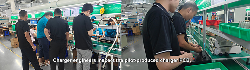
Once the electrical architecture is defined, engineers begin the PCB layout. This is where the theoretical circuit becomes a physical design.
For a charger, PCB layout is not simply about making all the components fit. Charger Engineers need to consider: Current paths, High-voltage spacing, Signal integrity, EMI, Heat generation, Component clearance, Transformer placement, USB-C port position, Grounding, Isolation and Safety requirements.
A small charger leaves very little room for mistakes.
Why PCB Layout Is Critical in GaN Chargers
GaN technology allows designers to achieve higher switching frequencies and power density. That is one reason modern GaN chargers can be significantly smaller than many traditional designs.
But higher power density also means the PCB has to be carefully designed.
Poor layout can contribute to:
• Excessive EMI
• Higher temperatures
• Unstable operation
• Signal interference
• Reduced efficiency
• Difficult certification testing
The compact size that makes a GaN charger attractive also makes engineering more demanding.
This is one reason a GaN charger manufacturer needs strong PCB and power-electronics engineering rather than relying only on assembly capability.
High-Voltage and Low-Voltage Areas Need to Be Separated
A charger contains different electrical regions. The AC input side operates at dangerous mains voltage.
The USB output side is a low-voltage output section. These areas need appropriate electrical separation.
Factory Charger Engineers need to consider: Creepage distance, Clearance, Insulation, Slot design, Component spacing, Transformer isolation, PCB material and Safety requirements.
These details may not be visible once the charger is assembled. But they are fundamental to the product's safety.
Step 4: Design the Thermal System at the Same Time
Thermal management should not be left until the end. This is a common mistake in product development.
Imagine the engineering team first designs a very small 100W charger. Later they discover that the internal temperature is too high.
At that point, simply “adding cooling” may not be possible.
The housing is already fixed.
The PCB is already designed.
The component positions may already be locked.
The result could be a much more expensive redesign.
A better approach is to consider thermal performance during the initial design.
Where Does Charger Heat Come From?
A charger is not 100% efficient, some electrical energy becomes heat.
Heat may originate from the charger's power switching operations, transformer losses, the rectification process, capacitors, inductors, PCB traces, protection components, and the USB-C port.
At low power, the heat may be manageable.
At 100W or 140W, even a small percentage of power loss can become significant.
For example, if a 100W charger has several watts of losses under a particular operating condition, those watts have to go somewhere.
The enclosure becomes part of the thermal system.
Why Charger Size and Power Are Closely Connected
A customer may ask: “Can you make the 100W charger smaller?”
Sometimes the answer is yes.
But not without engineering trade-offs.
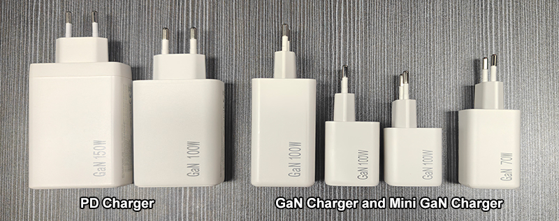
Reducing size implies, first and foremost, increased costs; additionally, it necessitates addressing higher power densities, elevated component temperatures, reduced component spacing, shortened heat dissipation paths, and increased complexity in PCB layout.
Gallium nitride (GaN) technology offers advantages, but its adoption does not eliminate the need for thermal design; rather, it provides charger engineers with greater design flexibility.
The final product still requires rigorous validation.
Step 5: Build the First Prototype
After the initial PCB design is completed, the first engineering samples can be built.
This is an exciting stage as the design begins to transform into a physical product, but do not mistake the initial prototype for the final charger.
It is a learning tool.
Manufacturer Engineers use it to discover what the computer models and design calculations cannot completely predict.
The prototype can reveal:
• Unexpected heat
• Mechanical interference
• EMI problems
• PD negotiation issues
• Noise
• Component stress
• Assembly difficulties
This is normal.
A good engineering process expects the first prototype to lead to improvements.
Prototype Testing Is More Than “Does It Charge?”
One of the simplest tests is connecting a device and checking whether it charges.
That is useful. It is not enough.
Engineers also need to check:
Output Voltage — Is the voltage stable?
Output Current — Can the charger deliver the required current?
Efficiency — How much input power is converted into useful output?
Temperature — Which components become hottest?
PD Negotiation — Does the charger communicate correctly?
Protection — Does the charger respond properly to abnormal conditions?
Mechanical Fit — Do the PCB, housing and ports fit correctly?
A charger can pass the first charging test and still fail several of these other checks.
Step 6: Test Under Different Loads
A charger should not only be tested at one convenient load.
Engineers may test: No load, Light load, Medium load, Full load, Rapid load changes, and Long-duration load.
This is particularly important for high-power products.
A 100W charger may work perfectly for five minutes. The more important question is: What happens after several hours of continuous operation?
Long-duration testing can reveal thermal problems and component instability that short tests may miss.
Step 7: Validate USB-C PD and PPS
This stage connects directly with the previous article on PD protocol tuning (This section discusses the working principle of PD protocol tuning in custom charger development). For a USB-C PD charger, engineers need to verify:
• Advertised power profiles
• Requested power
• Voltage transitions
• Current behavior
• PPS operation
• Device compatibility
• Cable behavior
• Multi-port power allocation
A 65W or 100W charger should be tested against the target devices defined during the product requirement stage.
This is particularly important for OEM products. A customer may have a target device list. The engineering team should test against that list rather than assuming generic compatibility.
Why Real Devices Still Matter
While engineering test equipment can provide precise measurement data, only the actual equipment reflects true operational performance.
Professional testing solutions cover smartphones, tablets, laptops, monitors, USB-C hubs, accessories, and more.
Different devices can negotiate power differently. This is one reason a USB-C charger factory with practical compatibility-testing experience can be valuable to an OEM buyer.
The product needs to work in the real world, not only on the laboratory bench.
Step 8: Mechanical Design and Housing Development
Electrical engineering and mechanical engineering now need to work closely together.
The housing needs to accommodate: PCB + Transformer + Capacitors + USB ports + Plug structure + Insulation + Heat dissipation + Mechanical supports.
For a custom charger, the customer may also want: Custom color, Logo, Surface finish, New housing shape, Retractable plug, Ultra-slim or mini size, and Custom packaging.
These changes can affect the internal engineering.A new housing is not always just a cosmetic change.
Why Custom Housing Can Affect the PCB
Imagine a customer asks for a thinner charger. The engineering team need to:
• Change PCB orientation
• Move the transformer
• Reduce component height
• Change connector placement
• Modify the heat path
• Rework insulation spacing
This is why experienced OEM manufacturers usually develop the electrical and mechanical design together.
A beautiful housing is useless if the electronics cannot operate safely inside it.
Step 9: Design for Manufacturing
At some point, the engineering question changes.
Instead of asking: “Can we make one working sample?”, the team needs to ask: “Can we make thousands of identical samples?”
This is the beginning of Design for Manufacturing, or DFM thinking. The engineering team reviews:
• Component placement
• SMT feasibility
• Soldering
• Assembly sequence
• Housing assembly
• Connector installation
• Testing access
• Production yield
• Inspection points
A prototype can be assembled slowly by experienced engineers. Mass production cannot depend on that.
Why a Prototype Is Not a Production Product
This difference is easy to overlook. During prototype development, an engineer may manually:
• Replace a component
• Modify a wire
• Adjust a PCB
• Rework solder joints
• Change a configuration
That may be acceptable during development. It is not acceptable as a normal mass-production process.
The final design needs to be stable enough for controlled manufacturing.
From Engineering Sample to DVT
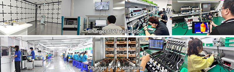
After the initial design has been improved, the product moves toward formal design validation.
DVT stands for: Design Validation Test.
The objective is to determine whether the design meets the defined requirements.
DVT include:
• Electrical testing
• Thermal testing
• Safety testing
• EMI/EMC
• PD compatibility
• Mechanical testing
• Drop testing
• Plug insertion testing
• Aging
• Reliability testing
The exact test list depends on the product and target market. The important point is that DVT is not simply another sample run.
It is a structured validation stage.
Imagine a 65W charger passes a basic functional test.
But during longer testing:
• The housing becomes too hot
• A component exceeds its temperature limit
• The USB-C port becomes unstable
• EMI performance is poor
If the factory goes directly into mass production, thousands of units could be affected. DVT creates an opportunity to identify these problems before the production volume becomes large.
That can save significant time and money.
Step 10: Tooling for the Final Housing
For a customized charger housing, tooling is another major milestone. The mold needs to reproduce the final design consistently.
Charger Engineers review: Wall thickness, Draft angles, Parting lines, Ejection, Tolerance, Surface finish, Assembly fit, Logo location, Plug mechanism.
A charger housing may appear simple, but the mold behind it is not necessarily so; even minute changes can affect fit and assembly.
Why Mold Development Should Happen After the Design Is Stable
Tooling is expensive to change. If the customer changes the product dimensions after the mold has already been produced, the project may need:
1.Mold modification
2.New samples
3.New fit testing
4.New mechanical validation
5.Additional cost
6.Additional lead time
This is why experienced OEM teams try to freeze the major mechanical and electrical requirements before committing to final tooling.
Step 11: PVT — Can the Factory Actually Produce It?
After design validation, the project moves toward: PVT — Production Validation Test.
This stage asks a different question from DVT.
DVT asks: Does the product design work?
PVT asks: Can the production process repeatedly make the product correctly?
That distinction is important. Even if a product has passed DVT, issues may still arise during actual manufacturing; PVT helps identify these problems.
Step 12: Production Line Setup
Before mass production begins, the factory needs to prepare the production process. Depending on the product, this include: SMT production → PCB inspection → Assembly stations → Functional testing → Hi-pot testing → Aging testing → Output testing → Visual inspection → Packaging.
The test procedures need to match the final product specification.
For example, if the charger supports multiple USB-C outputs, the production test should verify the relevant ports and power conditions.
Why Production Testing Matters
A good charger is not only one that passed engineering validation. It is a charger that can be produced consistently.
That means production quality control needs to catch issues such as: Wrong components, Poor solder joints, Incorrect assembly, Damaged housing, Port problems, Output abnormalities and Safety test failures.
This is one reason professional charger factories invest in automated inspection and testing.
From PCB to Mass Production: The Full Picture
The complete process can now be summarized:
1. Product Requirements
↓
2. Electrical Architecture
↓
3. Component Selection
↓
4. PCB Design
↓
5. Prototype
↓
6. Electrical + Thermal + PD Testing
↓
7. Mechanical Optimization
↓
8. DVT
↓
9. Tooling
↓
10. PVT
↓
11. Production Line Validation
↓
12. Mass Production
Each stage reduces a different type of risk.
What Can Go Wrong If the Process Is Too Short?
Some low-cost projects try to move directly from: Sample → Production, because it appears faster.
Sometimes it works.
Sometimes it creates much bigger problems later.
For example: poor thermal stability, PD compatibility issues, certification failure, high production defect rates, structural assembly problems, component shortages, inconsistent output performance, and so on.
A short development cycle is not always a faster project. If the product needs to be redesigned after mass production begins, the total project can take much longer.
Why Charger Engineering Experience Matters for OEM Chargers
This is especially important for B2B buyers. When sourcing a standard charger, the main questions may be: Price, MOQ, Lead time, Certification.
For a custom charger, the list becomes longer: Engineering, PCB design, Protocol, Thermal management, Mechanical design, Tooling, Validation, and Production.
The supplier needs to understand the complete chain. An experienced OEM charger manufacturer often offers far greater value than suppliers who can only provide low unit prices.
* OEM and ODM charger manufacturing
A 65W Charger Is a Good Example
Consider a customer developing a custom: 65W USB-C GaN charger
The project involve: GaN power architecture + USB-C PD + PPS + 65W output + Custom PCB + Compact housing + Thermal optimization + CB CE RoHS ERP certification + Custom logo + Custom packaging.
The charger may look like a relatively small product. But the engineering work behind it can involve several teams.
That is why a 65W charger factory should be evaluated on development capability, not only production price.(So this explains perfectly how to choose a 65W USB-C charger↗)
At 100W and 140W and above, PD 3.1/EPR and higher-power system design can add another level of complexity. The product may require more engineering work before it is ready for stable mass production.
What Should an OEM Buyer Ask the Factory?
Before starting a custom charger project, ask the manufacturer:
Engineering - Do you have an in-house R&D team?
PCB - Can you support PCB design and optimization?
Protocol - Can you customize PD/PPS parameters?
Thermal - Do you perform thermal analysis and testing?
Mechanical - Can you develop a custom housing?
Tooling - Do you manage mold development internally or through controlled suppliers?
Validation - Do you support EVT, DVT and PVT?
Production - Can the final design be manufactured at stable yield?
Certification - Can you support certification for the target market?
These questions can quickly separate an actual engineering manufacturer from a trading company.

ZONSAN has been focused on charger development and manufacturing since 2009, with products spanning USB chargers, GaN chargers, PD fast chargers, desktop chargers and other customized charging solutions. The company also presents OEM/ODM development as part of its B2B manufacturing service.
Its current product range covers multiple power levels, including 20W, 30W, 45W, 65W, 100W and 140W-class products, which means the engineering requirements can be addressed across different charger categories rather than relying on a single fixed platform.
For an OEM customer, the practical value is not simply having more products in a catalog.
It is having a development path that can move from: Requirement → Engineering → Prototype → Validation → Production, without handing every stage to a completely different supplier.
Final Thoughts
A charger may be small. The engineering process behind it is not.
From the first PCB layout to the final production line, a successful custom charger project requires many decisions to be made in the right order.
The PCB needs to work.
The PD protocol needs to communicate correctly.
The thermal system needs enough margin.
The housing needs to fit.
The product needs to pass validation.
And, perhaps most importantly, the factory needs to reproduce the same design consistently thousands of times.
That is the real difference between making a charger sample and developing a charger for mass production.
For brands looking for a custom charger manufacturer, the most useful question is therefore not simply: “How much does the charger cost?”
A better question is: “Can your engineering team take this product from PCB design to stable mass production?”
That answer tells you much more about the supplier's real capability.
FAQ
Q1: How long does it take to develop a custom charger?
The development time depends on the charger power, port configuration, protocol requirements, housing design and certification requirements. An existing platform can usually be developed faster than a completely new charger design.
Q2: What is the difference between a charger prototype and a production charger?
A prototype is mainly used to verify the design. A production charger must also be manufacturable, stable, certified and repeatable at volume.
Q3: What is DVT in charger development?
DVT stands for Design Validation Test. It verifies whether the charger design meets the required electrical, thermal, mechanical, safety and functional requirements.
Q4: What is PVT in charger manufacturing?
PVT stands for Production Validation Test. It checks whether the factory can consistently manufacture the approved charger design using the intended production process.
Q5: Can a charger factory design the PCB?
Yes. A capable OEM/ODM charger manufacturer can provide electrical architecture, PCB design, component selection, layout optimization and prototype development.
Q6: Why is PCB layout important in a GaN charger?
GaN chargers operate at high switching frequencies and high power density. PCB layout affects efficiency, thermal performance, EMI, isolation and overall stability.
Q7: Can a 65W charger be customized?
Yes. A 65W charger can be customized in areas such as port configuration, PD/PPS profiles, housing, plug type, branding, packaging and target-market certifications.
Q8: What is the difference between OEM and ODM charger development?
OEM development normally involves more customer-specific requirements, while ODM typically starts from an existing manufacturer platform that can be adapted to the customer's needs.
Q9: Can a 100W charger have multiple USB-C ports?
Yes. A 100W charger can be designed with multiple USB-C ports, but the total power and individual port outputs need to be clearly defined.
Q10: Why does charger development need thermal testing?
Electrical losses generate heat during operation. Thermal testing verifies that components and the enclosure remain within acceptable operating limits under different loads.
Q11: What should I ask a charger manufacturer before starting an OEM project?
Ask about R&D capability, PCB design, PD/PPS development, thermal testing, prototype support, DVT/PVT, certification, tooling, production capacity and quality control.
Q12: Can the same charger design be produced for different markets?
Often yes, but plug type, certification, input requirements, labeling and other market-specific requirements may need to be adjusted.
Reviewers by: Zonsan Sales Team and Engineers – Emma and Michael
Last Review Date: [September 02, 2026]