Inside ZONSAN’s Charger R&D Process
When a buyer looks at a finished USB-C charger, the product appears straightforward. There is a housing, a few ports, a plug, and a power rating printed on the label.
The engineering work behind it is much less visible.
Before a 65W GaN charger reaches mass production, for example, someone has to decide how the power architecture should work, which components are appropriate, how much heat the design can tolerate, how the PCB should be laid out, how the housing should accommodate the electronics, and how the finished product will be validated.
That work becomes even more complicated when the product is customized.
An OEM customer may want a different power profile, a smaller housing, a new port configuration, a different plug, a private mold, or support for a specific market certification.
At that point, the project is no longer simply about manufacturing an existing charger. It becomes an engineering project.
This is where the quality of a charger manufacturer's R&D process starts to matter.
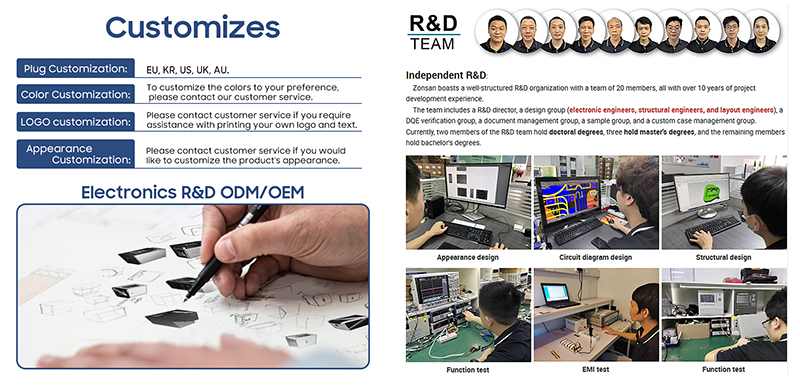
ZONSAN has developed chargers from 5W to 240W and maintains an R&D structure covering electronic engineering, structural design, layout engineering, validation and sample development. The company describes its R&D organization as including an R&D director, electronic and structural engineers, layout engineers, DQE validation, documentation, sample and custom-case teams.
So what actually happens before a new charger enters production?
Let's look inside the process.
Quick Answer: How Does ZONSAN Develop a New Charger?
ZONSAN's charger R&D process begins with customer requirements and product definition, followed by electrical architecture, PCB and layout development, structural and thermal engineering, prototype development, functional debugging, reliability validation, certification preparation, DVT/PVT and production transfer.
The important point is that these stages are connected.
A change in power output can affect the PCB.
A PCB change can affect thermal performance.
Thermal changes can affect the housing.
A housing change can affect tooling and certification.
Professional charger R&D is therefore not a straight line. It is a controlled engineering process in which different teams continuously verify whether the product is ready for the next stage.
1. Every Charger R&D Project Starts With a Product Requirement
The first step is not designing the PCB (Printed Circuit Board) layout. The primary task is to clearly define the charger's functional positioning and intended use.
For OEM or ODM projects(Understanding New Product Development), common initial requirements typically include target output power, number of ports, USB-C or USB-A interface configurations, PD/PPS/QC protocol specifications, target devices, plug type, housing dimensions, target markets, certification requirements, and target cost.
A 25W phone charger and a 140W laptop charger may both be called USB C chargers, but their engineering requirements are very different.
The same applies to the distinction between single-port chargers and multi-port desktop chargers. Therefore, the R&D team must clearly define the product before finalizing the technical approach.
This is an important part of OEM charger development because unclear requirements at the beginning often become engineering changes later.
2. Product Definition Connects the Commercial and Engineering Teams
A good charger R&D process has to translate commercial requirements into technical requirements.
A buyer might say: “We need a compact 65W charger for the European market.” That is a commercial requirement.
The engineering team then needs to turn it into technical questions.
How compact? Which ports? What PD profiles? Is PPS required?
What plug configuration? What operating temperature? What certification?
What type of housing? What level of thermal margin is required?
What is the estimated quantity?
This translation step is easy to overlook, but it is one of the most important parts of product development.
A professional charger manufacturer should not immediately promise a specification without first checking whether the requirements work together.
3. Electrical Architecture Comes Before PCB Layout
Once the requirements are defined, engineers can start developing the electrical architecture. This is where the fundamental power-conversion strategy is established.
Depending on the specific product, the R&D team may evaluate factors such as the charger's power requirements, internal components and structural design, charging protocols, and compliance with certification testing standards.
The goal is not simply to make the charger produce the advertised wattage.
The architecture needs to provide stable power while meeting safety, thermal, efficiency and certification requirements.
For high-power chargers, these decisions become particularly important because there is less room for engineering mistakes.
4. PCB Design Is Where Several Engineering Requirements Meet
After the electrical architecture is established, PCB development begins. PCB layout is not simply about fitting components onto a board.
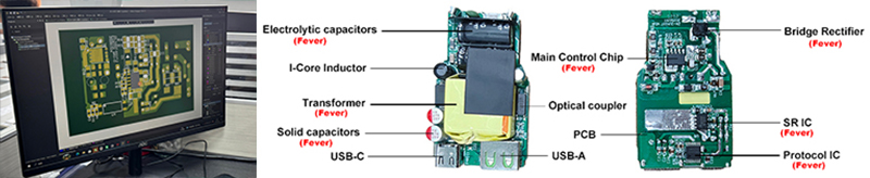
Engineers must consider numerous factors, such as current paths, component spacing, the separation of high- and low-voltage zones, signal routing, heat dissipation paths, transformer placement, electromagnetic interference (EMI), and creepage and clearance distances.
The PCB has to fit inside the intended housing while still providing enough electrical and thermal margin.
This becomes challenging in compact GaN chargers. The product may be physically small, but the internal power density is high.
A poor PCB layout can create problems that may not appear immediately during a short functional test.
It can contribute to excessive heat, EMI issues, inefficient power conversion or unstable operation.
This is why PCB engineering is one of the core capabilities of a serious USB-C charger manufacturer.
5. GaN Charger Development Requires a Different Level of Optimization
GaN technology has made it possible to build smaller and more power-dense chargers, but that does not mean GaN automatically makes charger development easier.
In fact, the opposite is often true.
When a charger becomes smaller and operates at higher switching frequencies, the engineering team has less physical space to manage:
• Heat, Electrical isolation, Component placemen;
• EMI, Power density, Mechanical tolerances.
ZONSAN's product development history includes compact GaN wall chargers from 20W through 65W as well as higher-power GaN desktop solutions up to 240W. Its current product development information specifically highlights high-power thermal design based on IEC 62368 requirements.
The challenge is not simply choosing a GaN device.
The complete power architecture has to be designed around it.
6. Structural Engineering Happens Alongside Electrical Engineering
The housing should not be treated as an afterthought.
The housing design(Check: Charger Housing Mold Development Process) should not be considered an afterthought. The charger's housing and dimensions determine the available space for the following components:
• PCB (Printed Circuit Board), transformers, capacitors, thermal interface materials, connectors, plug mechanisms, and insulation structures.
It also affects: heat dissipation (heat transfer), mechanical strength, port alignment, and plug stability.
For a customized charger, the electrical and structural teams therefore need to work together.
If the housing becomes smaller, the PCB may need to change.
If the PCB changes, component positions may change.
If component positions change, the thermal path may change.
That is why a professional custom charger manufacturer needs both electronic and structural engineering capability.
7. Thermal Design Is Part of the R&D Process, Not Just a Final Test
Thermal performance cannot be solved entirely at the end.
Engineers need to consider heat during the design stage.
Potential heat sources include: Power ICs, GaN devices, MOSFETs, Transformers,Rectifiers, and Other high-loss components.
The R&D team needs to understand where heat is generated and where it can go.
Possible solutions include:
• Component placement optimization and PCB copper optimization;
• Thermal pads and Internal thermal structures;
• Housing heat transfer and Reduced power losses.
This is particularly important for 100W, 140W and 240W charging platforms.
A charger that meets its electrical output but runs excessively hot under sustained load is not a finished engineering solution.
8. PD, PPS and Multi-Port Logic Are Validated During Development
Modern chargers increasingly support multiple charging protocols.
Depending on the product, this can include: USB-C PD, PPS, QC, Other device-specific charging requirements
For a single-port charger, the engineering challenge is relatively contained. For a multi-port charger, the power architecture becomes more complicated.
The charger may need to determine how available power is distributed when multiple devices are connected.
Example: a desktop charger might need to support a high-power USB-C port while simultaneously supplying lower-power outputs to other devices.
This means the R&D process has to validate not only individual ports, but also how the system behaves when those ports are used together.
9. Prototype Development Turns the Design Into a Physical Product
Once the electrical and mechanical designs are sufficiently mature, the project moves into prototype development.
This is an important transition.
On a computer screen, a design may look correct. A physical prototype can reveal things that simulation or drawings do not fully expose.
Engineers can inspect:
• Actual component spacing, Housing fit, Port alignment;
• Transformer position, Assembly feasibility, Thermal behavior;
• Plug structure, PCB-to-housing interaction.
Prototype development therefore provides an early opportunity to identify problems before they become expensive tooling or mass-production problems.
10. Engineering Debugging Is Where the Design Gets Refined
The first prototype is rarely the final product.
Engineers may also need to debug the charger, covering aspects such as output voltage, load characteristics, PD negotiation, and PPS operation, as well as protection functions, temperature, EMI (electromagnetic interference), power efficiency, and port characteristics.
This is normal.
Engineering development is not about producing a perfect first sample. It is about finding problems early enough to fix them.
The quality of a charger R&D team is often reflected in how systematically it handles these problems.
A strong team records the issue, identifies the cause, makes a controlled change, and verifies the result. It does not simply change components until the sample happens to work.
11. Validation Determines Whether the Prototype Is Ready to Move Forward
After debugging, the product needs structured validation.
This is where engineering moves from: "It works." to: "It works consistently under defined conditions."
Validation can include:
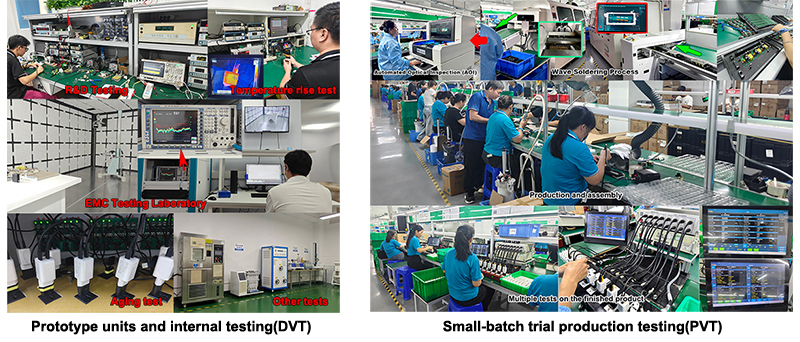
• Full-load testing, Temperature-rise testing, Input variation, Output stability;
• Protection testing, PD/PPS compatibility, Aging, Mechanical testing;
• Safety-related testing, Reliability testing.
The exact test program depends on the product and target market.
The purpose is the same: identify weaknesses before mass production.
12. DVT and PVT Turn Engineering Into a Production Process
For professional OEM development, product validation cannot stop with a successful prototype.
DVT, or Design Validation Testing, is used to verify whether the design meets its intended requirements.
PVT, or Production Validation Testing, goes one step further.
The question becomes whether the product can be manufactured consistently using the intended production process.
This distinction matters.
A charger may work perfectly when assembled by an engineer. That does not automatically mean the same performance will be achieved across thousands of production units.
PVT therefore connects R&D with manufacturing.
The production process, assembly method, inspection points and testing procedures all need to support the final design.
13. Certification Preparation Is Integrated Into Product Development
Certification is integrated into every stage of a charger project from the very beginning. Preparation for certification should not be viewed merely as a final administrative approval step; the design itself directly influences the certification outcome.
This is one reason why experienced charger manufacturers hold an advantage over suppliers who primarily coordinate external production.
From the initial design phase, engineers can factor in certification requirements and preparatory work, making informed decisions accordingly.
This reduces the risk of encountering setbacks during laboratory testing due to the need for major design modifications or other issues.
14. Engineering Documentation Keeps the Product Under Control
The charger development process involves not only producing PCBs (Printed Circuit Boards) but also generating various technical documents.
These documents may include circuit schematics, PCB files, bills of materials (BOM), engineering drawings, test records, specifications, sample records, engineering change records, and verification results.
Documentation may sound less interesting than the actual hardware, but it becomes extremely important once the product enters mass production.
If a component changes six months later, engineers need to know exactly what the original design contained.
If a customer requests a specification change, the team needs a controlled way to evaluate the impact.
This is part of maintaining product consistency.
15. Engineering Change Control Matters After Launch
The PD Gan charger's R&D process does not conclude when the product enters production.
Commercial products often require changes later.
For example:
• A component becomes obsolete.
• A supplier changes a component.
• A customer requests a new plug.
• A certification requirement changes.
• A housing needs modification.
• A new port configuration is requested.
The engineering team also needs to evaluate the changes to determine whether any adjustments or modifications to the charger will impact performance or certification.
This is why experienced manufacturers treat engineering changes as controlled processes rather than informal substitutions.

ZONSAN's R&D Structure Connects Design and Validation
One of the more important aspects of ZONSAN's R&D organization is that it is not presented simply as a group of PCB designers.
The Zonsan's published R&D structure includes electronic engineers, structural engineers, layout engineers, a DQE validation group, documentation management, sample development and custom-case management.
That structure reflects an important reality of charger development: A charger is a system, not a single circuit board.
Electrical performance, mechanical design, thermal behavior, validation and manufacturing all have to converge before a product is ready.
The ZONSAN R&D team has completed over 1,000 engineering projects and comprises 21 R&D engineers.
These figures are useful not because a larger team automatically means better products, but because they indicate that charger development is treated as an ongoing engineering activity rather than occasional product sourcing.
From R&D to Mass Production
Once validation is complete, the project moves toward production transfer.
At this point, the question changes again.
The R&D team has proven that the product works. Manufacturing now needs to prove that it can reproduce that result.
The transition can involve:
Final BOM → Production Documentation → Tooling / Fixtures → SMT Preparation → Assembly Process → Production Testing → Aging → Final QC → Mass Production.
ZONSAN's published production system includes incoming material inspection, plug-in inspection, semi-finished product testing, repair-welding inspection, aging testing, final electrical testing, appearance inspection and warehouse control. (Find out how USB-C chargers are made here.)
This connection between R&D and manufacturing is critical.
A strong prototype means little if the factory cannot reproduce it consistently.
Read More
What This Means for OEM Charger Buyers
For a buyer developing a customized charger, the R&D process should be one of the first things to investigate.
Do not only ask: “What models do you have?”
Also ask: “How do you develop a new model?”
A capable charger manufacturer should be able to explain:
• How requirements are reviewed
• Who designs the electrical architecture
• How PCB development is handled
• How structural design is integrated
• How thermal performance is evaluated
• How prototypes are tested
• How DVT/PVT are managed
• How certification is prepared
• How engineering changes are controlled
• How the design is transferred to mass production
These questions quickly reveal whether you are dealing with a true manufacturer with engineering capability or primarily a trading intermediary.
Why R&D Capability Matters More as Charger Power Increases
The higher the power, the less room there is for weak engineering.
At 20W, the design constraints are relatively manageable.
At 65W, thermal and power-density considerations become more important.
At 100W and above, the engineering relationship between power conversion, thermal design, PCB layout, component selection and safety becomes increasingly critical.
At 140W and 240W, the product is operating in a very different engineering environment from a basic phone charger.
This is why a buyer sourcing high-power GaN or PD3.1 chargers should evaluate the manufacturer's engineering team before focusing too heavily on unit price. (Learn more why charger engineering matters more than price.)
The product may look compact, but the engineering challenges behind it are anything but trivial.
What Makes a Good Charger R&D Process?
A strong charger R&D process has several characteristics.
It starts with requirements. The team understands what the customer actually needs before selecting a design.
It considers the whole product. Electrical, mechanical, thermal and manufacturing requirements are evaluated together.
It validates instead of assuming. Engineers test the physical product rather than relying only on design calculations.
It controls changes. Engineering modifications are documented and evaluated for their impact.
It connects R&D with production. The final design is developed with mass manufacturing in mind.
It learns from previous projects. Problems discovered in testing and production should feed back into future product development.
This last point is particularly important.
Excellent engineering teams do not start from scratch every time; they continuously build on their experience and innovate.
R&D Is What Allows a Charger Factory to Build More Than One Product
A factory with only production capability can manufacture a product.
A factory with strong R&D capability can develop product platforms.
That difference matters for brands with multiple charging products.
A successful engineering platform can support related products with different: Wattages, Port configurations, Housing designs, Plug types, Output profiles.
This can reduce duplicated development work and make future product launches more efficient.
For an OEM customer planning a product family rather than one isolated charger, this can be a major advantage.
Final Thoughts
A modern charger may be small enough to fit in the palm of your hand.
Its development process is anything but simple.
From the first product requirement to electrical architecture, PCB design, structural engineering, thermal optimization, prototype debugging, validation, certification preparation and production transfer, every stage affects the final product.
This is why the quality of a charger R&D process matters just as much as the production equipment itself.
For OEM and ODM buyers, the right question is not simply whether a factory can manufacture a charger.
The better question is whether the factory has the engineering system to develop, validate, improve and reproduce that charger consistently.
That is the difference between buying an existing product and working with a real charger manufacturing partner.
FAQ
Q1: What is the R&D process for a charger?
A typical charger R&D process includes product requirement definition, electrical architecture, PCB design, structural and thermal engineering, prototype development, debugging, validation, certification preparation, DVT/PVT and production transfer.
Q2: How long does charger R&D take?
The development time depends on whether the project uses an existing platform or requires a new electrical and mechanical design. A customized product with new tooling and certification generally requires more development time than a modified existing model.
Q3: What does a charger R&D engineer do?
Charger R&D engineers may work on power architecture, PCB design, component selection, thermal performance, USB-C PD/PPS behavior, protection circuits, testing and engineering changes.
Q4: Why is PCB design important in charger development?
PCB design affects electrical performance, thermal behavior, EMI, component placement, safety spacing and the ability to fit the electronics into a compact housing.
Q5: How are GaN chargers developed?
GaN charger development involves power architecture, high-frequency switching design, PCB layout, thermal management, component selection, PD/PPS integration, prototype testing and reliability validation.
Q6: What is DVT in charger development?
DVT, or Design Validation Testing, verifies whether the charger design meets its intended electrical, thermal, mechanical and functional requirements before production is finalized.
Q7: What is PVT in charger manufacturing?
PVT, or Production Validation Testing, verifies whether the validated charger design can be manufactured consistently using the intended production process.
Q8: Can a charger manufacturer customize the PCB?
A genuine OEM/ODM charger manufacturer with in-house engineering capability can develop or modify PCB and power architecture depending on the project requirements.
Q9: What is the difference between charger R&D and charger manufacturing?
R&D creates and validates the product design. Manufacturing reproduces the validated design consistently at production scale. A capable OEM factory needs both capabilities to support complex customization.
Q10: Why does charger R&D matter for OEM buyers?
Strong R&D reduces the risk of design problems, certification delays, thermal issues, compatibility problems and inconsistent mass production. It also gives brands more flexibility when developing customized charging products.
Reviewers: Zonsan R&D Engineer: Miller; Production Supervisor: Luo Zhang
Second Reviewers: Luke and Kelly
Final Review Date: [September 12, 2026]